- 您现在的位置:买卖IC网 > PDF目录17036 > EVAL-AD7262EDZ (Analog Devices Inc)BOARD EVAL CONTROL AD7262 PDF资料下载
参数资料
| 型号: | EVAL-AD7262EDZ |
| 厂商: | Analog Devices Inc |
| 文件页数: | 21/33页 |
| 文件大小: | 0K |
| 描述: | BOARD EVAL CONTROL AD7262 |
| 标准包装: | 1 |
| ADC 的数量: | 2 |
| 位数: | 12 |
| 采样率(每秒): | 1M |
| 数据接口: | 串行 |
| 输入范围: | 5 Vpp |
| 在以下条件下的电源(标准): | 120mW @ 1MSPS |
| 工作温度: | -40°C ~ 105°C |
| 已用 IC / 零件: | AD7262 |
| 已供物品: | 板,CD |
第1页第2页第3页第4页第5页第6页第7页第8页第9页第10页第11页第12页第13页第14页第15页第16页第17页第18页第19页第20页当前第21页第22页第23页第24页第25页第26页第27页第28页第29页第30页第31页第32页第33页
AD7262
Rev. 0 | Page 27 of 32
CALIBRATION
The AD7262/AD7262-5 registers store the offset value that can
be accessed easily by the user (see the Reading from a Register
section). When the device is calibrating, the differential analog
inputs for each respective ADC are shorted together internally
and a conversion is performed. A digital code representing the
offset is stored internally in the offset registers, and subsequent
conversion results have this measured offset removed.
INTERNAL OFFSET CALIBRATION
The AD7262/AD7262-5 allow the user to calibrate the device
offset using the CAL pin. This is achieved by setting the CAL
pin to a high logic level, which initiates a calibration on the next
CS falling edge. The calibration requires one full conversion
cycle, which contains a CS falling edge followed by 19 SCLKs to
complete. The CAL pin can remain high for more than one
conversion if desired, and the AD7262/AD7262-5 continue to
calibrate.
When the AD7262/AD7262-5 are calibrated, the calibration
results stored in the internal device registers are only relevant
for the particular PGA gain selected at the time of calibration. If
the PGA gain is changed, the AD7262/AD7262-5 must be
recalibrated. If the device is not recalibrated when the PGA gain
is changed, the offset for the previous gain setting continues to
be removed from the digital output code, which may lead to
inaccuracies.
The CAL pin should only be driven high when the CS pin is high
or after 19 SCLK cycles have elapsed when CS is low (that is,
between conversions). The CAL pin must be driven high t12 ns
before CS goes low. If the CS pin goes low before the t12 has
elapsed, the calibration result is inaccurate for the current
conversion, but, provided that the CAL pin remains high, the
subsequent calibration conversion is correct. If the CAL pin is
set to a logic high state during a conversion, that conversion result
is corrupted.
The offset range, which can be calibrated for, is ±128 least
significant bits at a gain of 1. The maximum offset voltage,
which can be calibrated for, is reduced as the gain of the PGA
is increased.
Provided that the CAL pin has been held high for a minimum
of one conversion, and once t12 and t11 have been adhered to, the
calibration is complete after the 19th SCLK cycle, and the CAL
pin can be driven to a logic low state. The next CS falling edge
after the CAL pin has been driven to a low logic state initiates
a conversion of the differential analog input signal for both
ADC A and ADC B.
Table 12 details the maximum offset voltage, which can be
removed by the AD7262/AD7262-5 without compromising the
available digital output code range. The least significant bit size is
AVCC/2BITs, which is 5/4096 or 1.22 mV for the
AD7262/
AD7262-5. The maximum removable offset voltage is
given by
Gain
mV
22
.
1
LSB
128
×
±
Table 12. Offset Range
Alternatively, one can use the control register to initiate an
offset calibration. This is done by setting the CAL bit in the
control register to 1. The calibration is then initiated on the next
CS falling edge, but the current conversion is corrupted. The
ADCs on the AD7262/AD7262-5 must remain fully powered
up to complete the internal calibration.
Gain
Maximum Removable Offset Voltage
1
±156.16 mV
2
±78.08 mV
3
±52.053 mV
32
±4.88 mV1
1 This is the maximum removable offset for PGA gain ≥ 32.
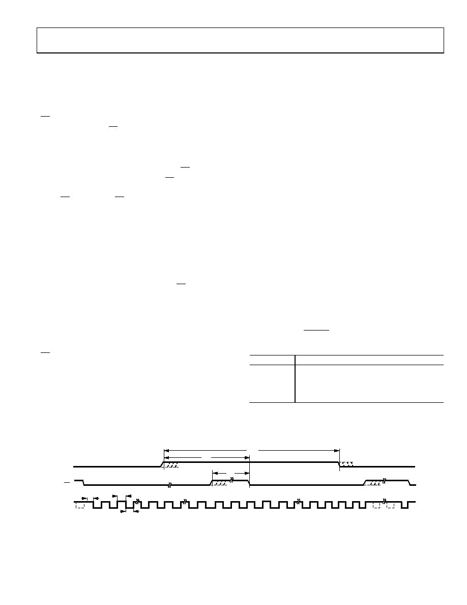
CS
SCLK
CAL
20
12
3
21
19
t2
t6
t8
t7
t12
t11
31
30
21
20
19
3
2
1
07
60
6-
03
6
Figure 36. Calibration Timing Diagram
相关PDF资料 |
PDF描述 |
|---|---|
| VE-212-EY | CONVERTER MOD DC/DC 15V 50W |
| EBC20DREH-S734 | CONN EDGECARD 40POS .100 EYELET |
| VE-J1P-EY | CONVERTER MOD DC/DC 13.8V 50W |
| EEC17DRAS-S734 | CONN EDGECARD 34POS .100 R/A PCB |
| VI-J1P-EY | CONVERTER MOD DC/DC 13.8V 50W |
相关代理商/技术参数 |
参数描述 |
|---|---|
| EVAL-AD7264EDZ | 功能描述:BOARD EVALUATION FOR AD7264 RoHS:是 类别:编程器,开发系统 >> 评估板 - 模数转换器 (ADC) 系列:- 产品培训模块:Obsolescence Mitigation Program 标准包装:1 系列:- ADC 的数量:1 位数:12 采样率(每秒):94.4k 数据接口:USB 输入范围:±VREF/2 在以下条件下的电源(标准):- 工作温度:-40°C ~ 85°C 已用 IC / 零件:MAX11645 已供物品:板,软件 |
| EVAL-AD7265CB | 制造商:AD 制造商全称:Analog Devices 功能描述:Differential/Single-Ended Input, Dual 1 MSPS, 12-Bit, 3-Channel SAR ADC |
| EVAL-AD7265CB1 | 制造商:AD 制造商全称:Analog Devices 功能描述:Differential Input, Dual 1 MSPS, 12-Bit, 3-Channel SAR ADC |
| EVAL-AD7265EDZ | 功能描述:BOARD EVAL FOR AD7265 A/D CONV RoHS:是 类别:编程器,开发系统 >> 评估板 - 模数转换器 (ADC) 系列:- 产品培训模块:Obsolescence Mitigation Program 标准包装:1 系列:- ADC 的数量:1 位数:12 采样率(每秒):94.4k 数据接口:USB 输入范围:±VREF/2 在以下条件下的电源(标准):- 工作温度:-40°C ~ 85°C 已用 IC / 零件:MAX11645 已供物品:板,软件 |
| EVAL-AD7266CB | 制造商:Analog Devices 功能描述:EVALUATION CONTROL BOARD I.C. - Bulk |
发布紧急采购,3分钟左右您将得到回复。