- 您现在的位置:买卖IC网 > PDF目录17060 > EVAL-AD7466CBZ (Analog Devices Inc)BOARD EVALUATION FOR AD7466 PDF资料下载
参数资料
| 型号: | EVAL-AD7466CBZ |
| 厂商: | Analog Devices Inc |
| 文件页数: | 10/29页 |
| 文件大小: | 0K |
| 描述: | BOARD EVALUATION FOR AD7466 |
| 标准包装: | 1 |
| ADC 的数量: | 1 |
| 位数: | 12 |
| 采样率(每秒): | 200k |
| 数据接口: | 串行 |
| 输入范围: | 0 ~ 3.6 V |
| 在以下条件下的电源(标准): | 0.9mW @ 100kSPS,3 V |
| 工作温度: | -40°C ~ 85°C |
| 已用 IC / 零件: | AD7466 |
| 已供物品: | 板,CD |
| 相关产品: | AD7466BRTZREEL7DKR-ND - IC ADC 12BIT 1.6V LP SOT23-6 AD7466BRTZ-R2-ND - IC ADC 12BIT 1.6V LP SOT23-6 AD7466BRMZ-REEL7-ND - IC ADC 12BIT 1.6V LP 8-MSOP AD7466BRTZ-REEL-ND - IC ADC 12BIT 1.6V LP SOT23-6 AD7466BRMZ-REEL-ND - IC ADC 12BIT 1.6V LP 8-MSOP AD7466BRTZREEL7CT-ND - IC ADC 12BIT 1.6V LP SOT23-6 AD7466BRTZREEL7TR-ND - IC ADC 12BIT 1.6V LP SOT23-6 AD7466BRMZ-ND - IC ADC 12BIT 1.6V LP 8-MSOP AD7466BRT-R2CT-ND - IC ADC 12BIT 1.6V LP SOT23-6 |
第1页第2页第3页第4页第5页第6页第7页第8页第9页当前第10页第11页第12页第13页第14页第15页第16页第17页第18页第19页第20页第21页第22页第23页第24页第25页第26页第27页第28页第29页
AD7466/AD7467/AD7468
Rev. C | Page 17 of 28
THEORY OF OPERATION
CIRCUIT INFORMATION
The AD7466/AD7467/AD7468 are fast, micropower, 12-bit,
10-bit, and 8-bit ADCs, respectively. The parts can be operated
from a 1.6 V to 3.6 V supply. When operated from any supply
voltage within this range, the AD7466/AD7467/AD7468 are
capable of throughput rates of 200 kSPS when provided with a
3.4 MHz clock.
The AD7466/AD7467/AD7468 provide the user with an on-
chip track-and-hold, an ADC, and a serial interface housed in a
tiny 6-lead SOT-23 or an 8-lead MSOP package, which offer the
user considerable space-saving advantages over alternative
solutions. The serial clock input accesses data from the part, but
also provides the clock source for the successive approximation
ADC. The analog input range is 0 V to VDD. An external refer-
ence is not required for the ADC, and there is no on-chip
reference. The reference for the AD7466/AD7467/AD7468 is
derived from the power supply, thus giving the widest possible
dynamic input range.
The AD7466/AD7467/AD7468 also feature an automatic
power-down mode to allow power savings between conversions.
The power-down feature is implemented across the standard
serial interface, as described in the Normal Mode section.
CONVERTER OPERATION
The AD7466/AD7467/AD7468 are successive approximation
analog-to-digital converters based around a charge redistribu-
of the ADC. Figure 19 shows the ADCs during the acquisition
phase. SW2 is closed and SW1 is in Position A, the comparator
is held in a balanced condition, and the sampling capacitor
acquires the signal on VIN.
SW2
SAMPLING
CAPACITOR
ACQUISITION
PHASE
COMPARATOR
CHARGE
REDISTRIBUTION
DAC
CONTROL
LOGIC
SW1
A
B
AGND
VIN
VDD/2
02643-020
Figure 19. ADC Acquisition Phase
When the ADC starts a conversion, as shown in Figure 20,
SW2 opens and SW1 moves to Position B, causing the com-
parator to become unbalanced. The control logic and the
charge redistribution DAC are used to add and subtract fixed
amounts of charge from the sampling capacitor to bring the
comparator back into a balanced condition. When the com-
parator is rebalanced, the conversion is complete. The control
logic generates the ADC output code. Figure 21 shows the ADC
transfer function.
SAMPLING
CAPACITOR
COMPARATOR
VIN
SW2
CONVERSION
PHASE
SW1
A
B
AGND
VDD/2
CHARGE
REDISTRIBUTION
DAC
CONTROL
LOGIC
02643-021
Figure 20. ADC Conversion Phase
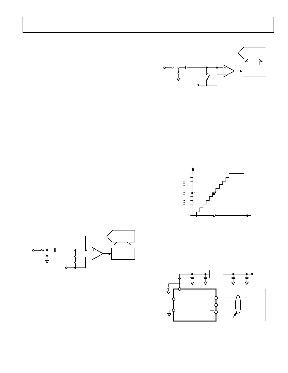
ADC TRANSFER FUNCTION
The output coding of the AD7466/AD7467/AD7468 is straight
binary. The designed code transitions occur at successive
integer LSB values; that is, 1 LSB, 2 LSB, and so on. The LSB size
for the devices is as follows:
VDD/4096 for the AD7466
VDD/1024 for the AD7467
VDD/256 for the AD7468
The ideal transfer characteristics for the devices are shown in
111...111
111...110
111...000
011...111
+VDD – 1LSB
0V 1LSB
ANALOG INPUT
ADC
CODE
1LSB = VDD/4096 (AD7466)
1LSB = VDD/1024 (AD7467)
1LSB = VDD/256 (AD7468)
000...010
000...001
000...000
02643-022
Figure 21. AD7466/AD7467/AD7468 Transfer Characteristics
TYPICAL CONNECTION DIAGRAM
Figure 22 shows a typical connection diagram for the devices.
VREF is taken internally from VDD and, therefore, VDD should
be well decoupled. This provides an analog input range of
0 V to VDD.
AD7466
SCLK
SDATA
VIN
GND
0V TO VDD
INPUT
VDD
0.1
μF
10
μF
μC/μP
0.1
μF
1
μF
TANT
REF192
240
μA
680nF
2.5V
5V
SUPPLY
SERIAL
INTERFACE
CS
02643-023
Figure 22. REF192 as Power Supply to AD7466
相关PDF资料 |
PDF描述 |
|---|---|
| RCM15DCCD-S189 | CONN EDGECARD 30POS R/A .156 SLD |
| EVAL-AD7739EBZ | BOARD EVAL FOR AD7739 |
| EEV-HA1H330UP | CAP ALUM 33UF 50V 20% SMD |
| VE-B3B-EY | CONVERTER MOD DC/DC 95V 50W |
| EVAL-AD7738EBZ | BOARD EVAL FOR AD7738 |
相关代理商/技术参数 |
参数描述 |
|---|---|
| EVAL-AD7467CB | 制造商:Analog Devices 功能描述:EVAL KIT FOR 1.6V, MICROPWR 12/10/8BIT ADCS - Bulk |
| EVAL-AD7470 | 制造商:AD 制造商全称:Analog Devices 功能描述:Evaluation Board for 10-/12-Bit High Speed, Low Power ADCs |
| EVAL-AD7470_07 | 制造商:AD 制造商全称:Analog Devices 功能描述:Evaluation Board for 10-/12-Bit High Speed, Low Power ADCs |
| EVAL-AD7470CB | 制造商:Analog Devices 功能描述:EVAL BD FOR AD7470 ADC - Bulk |
| EVAL-AD7470CB2 | 制造商:AD 制造商全称:Analog Devices 功能描述:1.75 MSPS, 4 mW 10-Bit/12-Bit Parallel ADCs |
发布紧急采购,3分钟左右您将得到回复。