- 您现在的位置:买卖IC网 > PDF目录17036 > EVAL-AD7682EDZ (Analog Devices Inc)BOARD EVAL AD7682 PDF资料下载
参数资料
| 型号: | EVAL-AD7682EDZ |
| 厂商: | Analog Devices Inc |
| 文件页数: | 22/32页 |
| 文件大小: | 0K |
| 描述: | BOARD EVAL AD7682 |
| 标准包装: | 1 |
| 系列: | PulSAR® |
| ADC 的数量: | 1 |
| 位数: | 16 |
| 采样率(每秒): | 250k |
| 数据接口: | 串行 |
| 输入范围: | ±VREF |
| 在以下条件下的电源(标准): | 12.5mW @ 250kSPS,5V |
| 工作温度: | -40°C ~ 85°C |
| 已用 IC / 零件: | AD7682 |
| 已供物品: | 板 |
第1页第2页第3页第4页第5页第6页第7页第8页第9页第10页第11页第12页第13页第14页第15页第16页第17页第18页第19页第20页第21页当前第22页第23页第24页第25页第26页第27页第28页第29页第30页第31页第32页
Data Sheet
AD7682/AD7689
Rev. D | Page 29 of 32
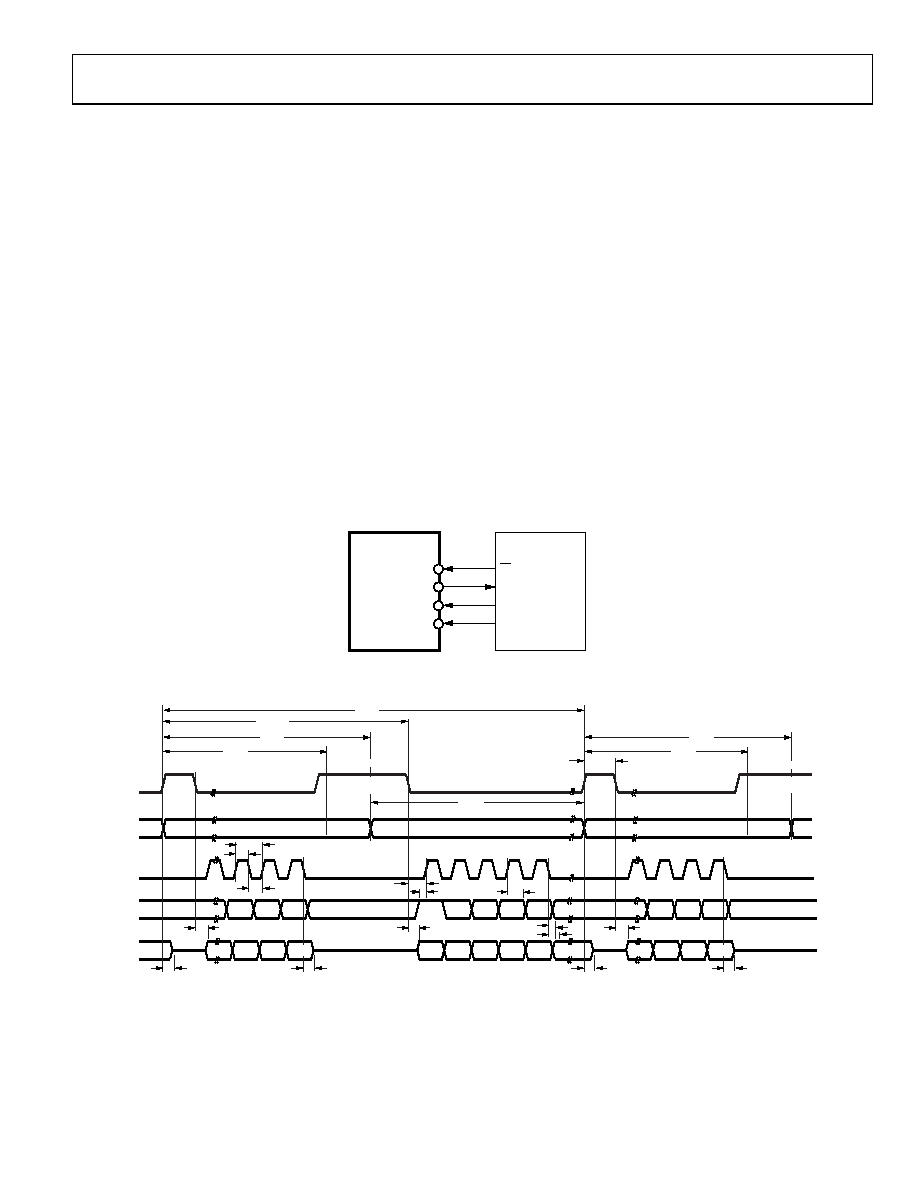
READ/WRITE SPANNING CONVERSION WITHOUT
A BUSY INDICATOR
to any host using an SPI, serial port, or FPGA. The connection
diagram is shown in Figure 40, and the corresponding timing
is given in Figure 41. For the SPI, the host should use CPHA =
CPOL = 0. Reading/writing spanning conversion is shown,
which covers all three modes detailed in the Digital Interface
section. For this mode, the host must generate the data transfer
based on the conversion time. For an interrupt driven transfer
that uses a busy indicator, refer to the Read/Write Spanning
Conversion with a Busy Indicator section.
A rising edge on CNV initiates a conversion, forces SDO to
high impedance, and ignores data present on DIN. After a
conversion is initiated, it continues until completion irrespec-
tive of the state of CNV. CNV must be returned high before the
safe data transfer time, tDATA, and then held high beyond the
conversion time, tCONV, to avoid generation of the busy signal
indicator.
the acquisition phase and power-down. When the host brings
CNV low after tCONV (maximum), the MSB is enabled on SDO.
The host also must enable the MSB of the CFG register at this
time (if necessary) to begin the CFG update. While CNV is low,
both a CFG update and a data readback take place. The first 14
SCK rising edges are used to update the CFG, and the first 15
SCK falling edges clock out the conversion results starting with
MSB 1. The restriction for both configuring and reading is
that they both must occur before the tDATA time of the next conver-
sion elapses. All 14 bits of CFG[13:0] must be written, or they
are ignored. In addition, if the 16-bit conversion result is not
read back before tDATA elapses, it is lost.
The SDO data is valid on both SCK edges. Although the rising
edge can be used to capture the data, a digital host using the
SCK falling edge allows a faster reading rate, provided it has an
acceptable hold time. After the 16th (or 30th) SCK falling edge, or
when CNV goes high (whichever occurs first), SDO returns to
high impedance.
If CFG readback is enabled, the CFG register associated with the
conversion result is read back MSB first following the LSB of the
conversion result. A total of 30 SCK falling edges is required to
return SDO to high impedance if this is enabled.
MISO
MOSI
SCK
SS
CNV
FOR SPI USE CPHA = 0, CPOL = 0.
SCK
SDO
DIN
AD7682/
AD7689
DIGITAL HOST
07
35
3-
03
6
UPDATE (n)
CFG/SDO
UPDATE (n + 1)
CFG/SDO
ACQUISITION (n)
ACQUISITION
(n + 1)
ACQUISITION
(n - 1)
MSB MSB – 1
1
2
BEGIN DATA (n – 1)
BEGIN CFG (n + 1)
CFG
MSB
CFG
MSB – 1
LSB + 1
14
15
SEE NOTE
NOTES
1. THE LSB IS FOR CONVERSION RESULTS OR THE CONFIGURATION REGISTER CFG (n – 1) IF
15 SCK FALLING EDGES = LSB OF CONVERSION RESULTS.
29 SCK FALLING EDGES = LSB OF CONFIGURATION REGISTER.
ON THE 16TH OR 30TH SCK FALLING EDGE, SDO IS DRIVEN TO HIGH IMPENDANCE.
16/
30
CONVERSION (n)
END DATA (n – 1)
END CFG (n + 1)
CFG
LSB
X
>
tCONV
LSB
SCK
CNV
DIN
SDO
LSB + 1
14
15
16/
30
CONVERSION (n – 1)
END DATA (n – 2)
END CFG (n)
CFG
LSB
X
tCONV
tDATA
tCNVH
tDATA
tDIS
tEN
tDSDO
tHSDO
tHDIN
tSDIN
tCLSCK
tEN
tSCK
tSCKH
tSCKL
tDIS
tCONV
LSB
07
35
3-
0
37
tACQ
tCYC
(QUIET
TIME)
(QUIET
TIME)
EOC
RETURN CNV HIGH
FOR NO BUSY
RETURN CNV HIGH
FOR NO BUSY
相关PDF资料 |
PDF描述 |
|---|---|
| LGU2E331MELZ | CAP ALUM 330UF 250V 20% SNAP |
| EVAL-AD7982SDZ | BOARD EVAL FOR AD7982 |
| VI-J1L-EY | CONVERTER MOD DC/DC 28V 50W |
| VE-21L-EY | CONVERTER MOD DC/DC 28V 50W |
| DC1009A-A | BOARD DELTA SIGMA ADC LTC2492 |
相关代理商/技术参数 |
参数描述 |
|---|---|
| EVAL-AD7683CB | 制造商:AD 制造商全称:Analog Devices 功能描述:16-Bit, 100 kSPS PulSAR ADC in MSOP/QFN |
| EVAL-AD7683CBZ | 制造商:Analog Devices 功能描述:EVAL BOARD 18BIT 100ksps I.C. |
| EVAL-AD7683SDZ | 功能描述:数据转换 IC 开发工具 EVAL BOARD 18BIT 100ksps I.C. RoHS:否 制造商:Texas Instruments 产品:Demonstration Kits 类型:ADC 工具用于评估:ADS130E08 接口类型:SPI 工作电源电压:- 6 V to + 6 V |
| EVAL-AD7684CBZ | 功能描述:BOARD EVALUATION FOR AD7684 RoHS:是 类别:编程器,开发系统 >> 评估板 - 模数转换器 (ADC) 系列:PulSAR® 产品培训模块:Obsolescence Mitigation Program 标准包装:1 系列:- ADC 的数量:1 位数:12 采样率(每秒):94.4k 数据接口:USB 输入范围:±VREF/2 在以下条件下的电源(标准):- 工作温度:-40°C ~ 85°C 已用 IC / 零件:MAX11645 已供物品:板,软件 |
| EVAL-AD7685CB | 制造商:Analog Devices 功能描述:Evaluation Board For Use With Either The Analog Devices 制造商:Analog Devices 功能描述:EVAL FOR AD7685 - Bulk 制造商:Rochester Electronics LLC 功能描述:EVAL FOR AD7685 - Bulk |
发布紧急采购,3分钟左右您将得到回复。