- 您现在的位置:买卖IC网 > PDF目录17044 > EVAL-AD7690SDZ (Analog Devices Inc)BOARD EVAL FOR AD7690 PDF资料下载
参数资料
| 型号: | EVAL-AD7690SDZ |
| 厂商: | Analog Devices Inc |
| 文件页数: | 6/24页 |
| 文件大小: | 0K |
| 描述: | BOARD EVAL FOR AD7690 |
| 标准包装: | 1 |
| 系列: | PulSAR® |
| ADC 的数量: | 1 |
| 位数: | 18 |
| 采样率(每秒): | 400k |
| 数据接口: | DSP,MICROWIRE?,QSPI?,串行,SPI? |
| 输入范围: | ±VREF |
| 在以下条件下的电源(标准): | 17mW @ 100kSPS |
| 工作温度: | -40°C ~ 85°C |
| 已用 IC / 零件: | AD7690 |
| 已供物品: | 板 |
AD7690
Rev. B | Page 14 of 24
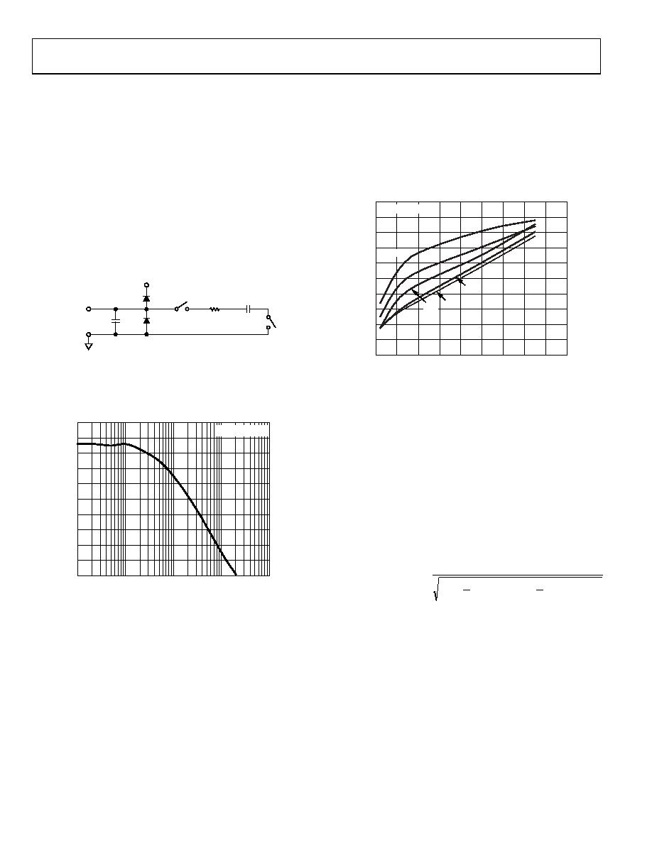
ANALOG INPUTS
Figure 27 shows an equivalent circuit of the input structure of
the AD7690.
The two diodes, D1 and D2, provide ESD protection for the
analog inputs, IN+ and IN. Care must be taken to ensure that
the analog input signal does not exceed the supply rails by more
than 0.3 V because this causes the diodes to become forward
biased and start conducting current. These diodes can handle a
forward-biased current of 130 mA maximum. For instance, these
conditions could eventually occur when the input buffer’s (U1)
supplies are different from VDD. In such a case (for example, an
input buffer with a short circuit), the current limitation can be
used to protect the part.
CIN
RIN
D1
D2
CPIN
IN+
OR IN–
GND
VDD
05
79
2-
00
9
Figure 27. Equivalent Analog Input Circuit
The analog input structure allows the sampling of the true
differential signal between IN+ and IN. By using these
differential inputs, signals common to both inputs are rejected.
90
40
1
10000
FREQUENCY (kHz)
CM
R
(
d
B)
05
79
2-
03
6
10
100
1000
85
80
75
70
65
60
55
50
45
VREF = VDD = 5V
Figure 28. Analog Input CMRR vs. Frequency
During the acquisition phase, the impedance of the analog
inputs (IN+ and IN) can be modeled as a parallel combination
of the capacitor, CPIN, and the network formed by the series
connection of RIN and CIN. CPIN is primarily the pin capacitance.
RIN is typically 600 Ω and is a lumped component composed
of serial resistors and the on resistance of the switches. CIN is
typically 30 pF and is mainly the ADC sampling capacitor.
During the conversion phase, where the switches are opened,
the input impedance is limited to CPIN. RIN and CIN make a 1-
pole, low-pass filter that reduces undesirable aliasing effects and
limits the noise.
When the source impedance of the driving circuit is low, the
AD7690 can be driven directly. Large source impedances
significantly affect the ac performance, especially total
harmonic distortion (THD). The dc performances are less
sensitive to the input impedance. The maximum source
impedance depends on the amount of THD that can be
tolerated. The THD degrades as a function of the source
impedance and the maximum input frequency.
05
79
2-
0
47
FREQUENCY (kHz)
T
HD
(
d
B
)
09
–130
–125
–120
–115
–110
–105
–100
–95
–90
–85
–80
10
20
30
40
50
60
70
80
0
33
100
15
VREF = VDD 5V
250
50
Figure 29. THD vs. Analog Input Frequency and Source Resistance
DRIVER AMPLIFIER CHOICE
Although the AD7690 is easy to drive, the driver amplifier must
meet the following requirements:
The noise generated by the driver amplifier must be kept
as low as possible to preserve the SNR and transition noise
performance of the AD7690. The noise from the driver is
filtered by the AD7690 analog input circuit’s 1-pole, low-
pass filter made by RIN and CIN or by the external filter,
if one is used. Because the typical noise of the AD7690 is
28 μV rms, the SNR degradation due to the amplifier is
+
=
+
2
dB
3
2
dB
3
2
)
(
2
π
)
(
2
π
28
log
20
N
LOSS
Ne
f
Ne
f
SNR
where:
f3 dB is the input bandwidth in megahertz of the AD7690
(9 MHz) or the cutoff frequency of the input filter, if one is
used.
N is the noise gain of the amplifier (for example, 1 in
buffer configuration).
eN+ and eN are the equivalent input noise voltage densities
of the op amps connected to IN+ and IN, in nV/√Hz.
This approximation can be used when the resistances
around the amplifiers are small. If larger resistances are
used, their noise contributions should also be root
summed squared.
相关PDF资料 |
PDF描述 |
|---|---|
| 0210490944 | CABLE JUMPER 1.25MM .051M 25POS |
| EVAL-AD7980SDZ | BOARD EVAL FOR AD7980 |
| PH50S2412 | CONVERTER DC/DC 12V 50W 6-PIN |
| 1624094-9 | INDUCTOR 220UH 100MA 1812 |
| EVAL-AD7685SDZ | BOARD EVAL FOR AD7685 |
相关代理商/技术参数 |
参数描述 |
|---|---|
| EVAL-AD7691CBZ | 功能描述:BOARD EVALUATION FOR AD7691CBZ RoHS:是 类别:编程器,开发系统 >> 评估板 - 模数转换器 (ADC) 系列:PulSAR® 产品培训模块:Obsolescence Mitigation Program 标准包装:1 系列:- ADC 的数量:1 位数:12 采样率(每秒):94.4k 数据接口:USB 输入范围:±VREF/2 在以下条件下的电源(标准):- 工作温度:-40°C ~ 85°C 已用 IC / 零件:MAX11645 已供物品:板,软件 |
| EVAL-AD7691SDZ | 功能描述:BOARD EVAL FOR AD7691 RoHS:是 类别:编程器,开发系统 >> 评估板 - 模数转换器 (ADC) 系列:PulSAR® 产品培训模块:Obsolescence Mitigation Program 标准包装:1 系列:- ADC 的数量:1 位数:12 采样率(每秒):94.4k 数据接口:USB 输入范围:±VREF/2 在以下条件下的电源(标准):- 工作温度:-40°C ~ 85°C 已用 IC / 零件:MAX11645 已供物品:板,软件 |
| EVAL-AD7693CB | 制造商:Analog Devices 功能描述:EVAL KIT FOR 16BIT, 0.5 LSB, 500 KSPS PULSARDIFFERENTIAL ADC - Bulk |
| EVAL-AD7693CBZ | 功能描述:BOARD EVALUATION FOR AD7693 RoHS:是 类别:编程器,开发系统 >> 评估板 - 模数转换器 (ADC) 系列:PulSAR® 产品培训模块:Obsolescence Mitigation Program 标准包装:1 系列:- ADC 的数量:1 位数:12 采样率(每秒):94.4k 数据接口:USB 输入范围:±VREF/2 在以下条件下的电源(标准):- 工作温度:-40°C ~ 85°C 已用 IC / 零件:MAX11645 已供物品:板,软件 |
| EVAL-AD7693SDZ | 功能描述:数据转换 IC 开发工具 EVAL BOARD 16-bit ADC 500kSPS RoHS:否 制造商:Texas Instruments 产品:Demonstration Kits 类型:ADC 工具用于评估:ADS130E08 接口类型:SPI 工作电源电压:- 6 V to + 6 V |
发布紧急采购,3分钟左右您将得到回复。