- 您现在的位置:买卖IC网 > PDF目录17044 > EVAL-AD7691SDZ (Analog Devices Inc)BOARD EVAL FOR AD7691 PDF资料下载
参数资料
| 型号: | EVAL-AD7691SDZ |
| 厂商: | Analog Devices Inc |
| 文件页数: | 6/28页 |
| 文件大小: | 0K |
| 描述: | BOARD EVAL FOR AD7691 |
| 标准包装: | 1 |
| 系列: | PulSAR® |
| ADC 的数量: | 1 |
| 位数: | 18 |
| 采样率(每秒): | 250k |
| 数据接口: | 串行 |
| 输入范围: | ±VREF |
| 在以下条件下的电源(标准): | 10.6mW @ 250kSPS,5 V |
| 工作温度: | -40°C ~ 85°C |
| 已用 IC / 零件: | AD7691 |
| 已供物品: | 板 |
第1页第2页第3页第4页第5页当前第6页第7页第8页第9页第10页第11页第12页第13页第14页第15页第16页第17页第18页第19页第20页第21页第22页第23页第24页第25页第26页第27页第28页
AD7691
Data Sheet
Rev. C | Page 14 of 28
THEORY OF OPERATION
SW+
MSB
65,536C
IN+
LSB
COMP
CONTROL
LOGIC
SWITCHES CONTROL
BUSY
OUTPUT CODE
CNV
REF
GND
IN–
4C
2C
C
131,072C
SW–
MSB
65,536C
LSB
4C
2C
C
131,072C
0
61
46
-02
4
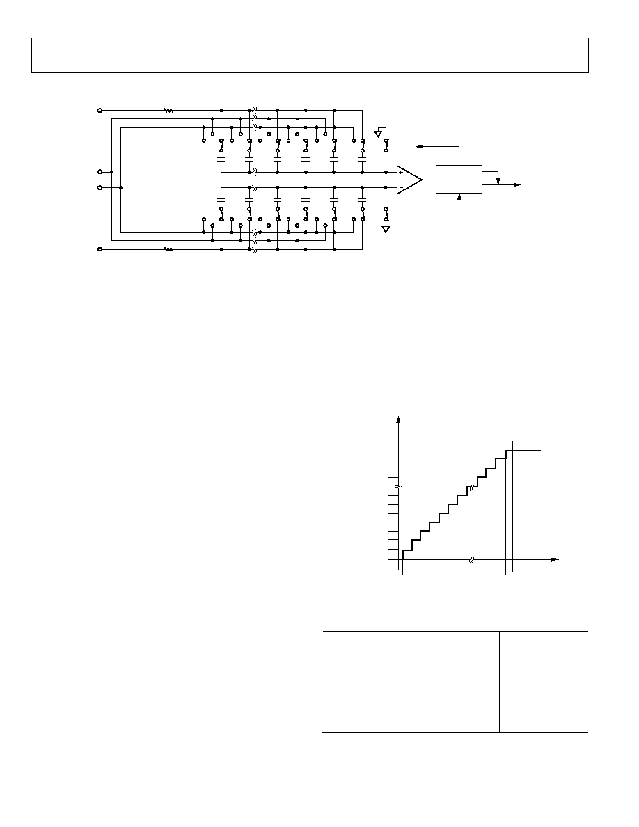
Figure 27. ADC Simplified Schematic
CIRCUIT INFORMATION
The AD7691 is a fast, low power, single-supply, precise, 18-bit
ADC using a successive approximation architecture.
The part is capable of converting 250,000 samples per second
(250 kSPS) and powers down between conversions. When
operating at 1 kSPS, for example, it consumes 50 μW typically,
which is ideal for battery-powered applications.
The AD7691 provides the user with an on-chip track-and-hold
and does not exhibit pipeline delay or latency, making it ideal
for multiple multiplexed channel applications.
The AD7691 is specified from 2.3 V to 5.25 V and can be
interfaced to any 1.8 V to 5 V digital logic family. It is housed in
a 10-lead MSOP or a tiny 10-lead QFN (LFCSP) that combines
space savings and allows flexible configurations.
The part is pin-for-pin compatible with the 18-bit AD7690 as
well as the 16-bit AD7687 and AD7688.
CONVERTER OPERATION
The AD7691 is a successive approximation ADC based on a
charge redistribution DAC. Figure 27 shows the simplified
schematic of the ADC. The capacitive DAC consists of two
identical arrays of 18 binary-weighted capacitors, which are
connected to the two comparator inputs.
During the acquisition phase, terminals of the array tied to the
comparator’s input are connected to GND via SW+ and SW.
All independent switches are connected to the analog inputs.
Thus, the capacitor arrays are used as sampling capacitors and
acquire the analog signal on the IN+ and IN inputs. When the
acquisition phase is complete and the CNV input goes high, a
conversion phase is initiated. When the conversion phase
begins, SW+ and SW are opened first. The two capacitor
arrays are then disconnected from the inputs and connected to
the GND input. Therefore, the differential voltage between the
inputs IN+ and IN captured at the end of the acquisition phase
is applied to the comparator inputs, causing the comparator to
become unbalanced. By switching each element of the capacitor
array between GND and REF, the comparator input varies by
binary-weighted voltage steps (VREF/2, VREF/4 ... VREF/262,144).
The control logic toggles these switches, starting with the MSB,
to bring the comparator back into a balanced condition. After
the completion of this process, the part returns to the
acquisition phase, and the control logic generates the ADC
output code and a busy signal indicator.
Because the AD7691 has an on-board conversion clock, the
serial clock, SCK, is not required for the conversion process.
Transfer Functions
The ideal transfer characteristic for the AD7691 is shown in
100...000
100...001
100...010
011...101
011...110
011...111
A
D
C
CO
DE
(T
W
O
S
CO
M
P
L
E
M
E
NT
)
ANALOG INPUT
+FSR – 1.5LSB
+FSR – 1LSB
–FSR + 1LSB
–FSR
–FSR + 0.5LSB
06
14
6-
0
06
Figure 28. ADC Ideal Transfer Function
Table 9. Output Codes and Ideal Input Voltages
Description
Analog Input
VREF = 5 V
Digital Output
Code (Hex)
FSR 1 LSB
+4.999962 V
Midscale + 1 LSB
+38.15 μV
0x00001
Midscale
0 V
0x00000
Midscale 1 LSB
38.15 μV
0x3FFFF
FSR + 1 LSB
4.999962 V
0x20001
FSR
5 V
1 This is also the code for an overranged analog input (VIN+ VIN above VREF VGND).
2 This is also the code for an underranged analog input (VIN+ VIN below VGND).
相关PDF资料 |
PDF描述 |
|---|---|
| STD12W-W | WIRE & CABLE MARKERS |
| REC5-0505SRW/H6/A | CONV DC/DC 5W 4.5-9VIN 05VOUT |
| RCM15DRMN | CONN EDGECARD 30POS .156 WW |
| STD12W-S | WIRE & CABLE MARKERS |
| ADR425ARMZ-REEL7 | IC VREF SERIES PREC 5V 8-MSOP |
相关代理商/技术参数 |
参数描述 |
|---|---|
| EVAL-AD7693CB | 制造商:Analog Devices 功能描述:EVAL KIT FOR 16BIT, 0.5 LSB, 500 KSPS PULSARDIFFERENTIAL ADC - Bulk |
| EVAL-AD7693CBZ | 功能描述:BOARD EVALUATION FOR AD7693 RoHS:是 类别:编程器,开发系统 >> 评估板 - 模数转换器 (ADC) 系列:PulSAR® 产品培训模块:Obsolescence Mitigation Program 标准包装:1 系列:- ADC 的数量:1 位数:12 采样率(每秒):94.4k 数据接口:USB 输入范围:±VREF/2 在以下条件下的电源(标准):- 工作温度:-40°C ~ 85°C 已用 IC / 零件:MAX11645 已供物品:板,软件 |
| EVAL-AD7693SDZ | 功能描述:数据转换 IC 开发工具 EVAL BOARD 16-bit ADC 500kSPS RoHS:否 制造商:Texas Instruments 产品:Demonstration Kits 类型:ADC 工具用于评估:ADS130E08 接口类型:SPI 工作电源电压:- 6 V to + 6 V |
| EVAL-AD7694CB | 制造商:Analog Devices 功能描述: |
| EVAL-AD7694CB1 | 制造商:AD 制造商全称:Analog Devices 功能描述:16-Bit, 250 kSPS PulSAR ADC in MSOP |
发布紧急采购,3分钟左右您将得到回复。