- 您现在的位置:买卖IC网 > PDF目录17044 > EVAL-AD7691SDZ (Analog Devices Inc)BOARD EVAL FOR AD7691 PDF资料下载
参数资料
| 型号: | EVAL-AD7691SDZ |
| 厂商: | Analog Devices Inc |
| 文件页数: | 8/28页 |
| 文件大小: | 0K |
| 描述: | BOARD EVAL FOR AD7691 |
| 标准包装: | 1 |
| 系列: | PulSAR® |
| ADC 的数量: | 1 |
| 位数: | 18 |
| 采样率(每秒): | 250k |
| 数据接口: | 串行 |
| 输入范围: | ±VREF |
| 在以下条件下的电源(标准): | 10.6mW @ 250kSPS,5 V |
| 工作温度: | -40°C ~ 85°C |
| 已用 IC / 零件: | AD7691 |
| 已供物品: | 板 |
第1页第2页第3页第4页第5页第6页第7页当前第8页第9页第10页第11页第12页第13页第14页第15页第16页第17页第18页第19页第20页第21页第22页第23页第24页第25页第26页第27页第28页
AD7691
Data Sheet
Rev. C | Page 16 of 28
DRIVER AMPLIFIER CHOICE
Although the AD7691 is easy to drive, the driver amplifier must
meet the following requirements:
The noise generated by the driver amplifier needs to be kept as
low as possible to preserve the SNR and transition noise
performance of the AD7691. The noise coming from the
driver is filtered by the AD7691 analog input circuit’s
1-pole, low-pass filter made by RIN and CIN or by the
external filter, if one is used. The SNR degradation due to
the amplifier is as follows:
SNRLOSS =
+
+
2
dB
3
2
dB
3
2
)
(
2
π
)
(
2
π
log
20
N
NADC
Ne
f
Ne
f
V
where:
VNADC is the noise of the ADC, in μV, given by the following:
20
10
2
SNR
INpp
NADC
V
=
f3dB is the input bandwidth, in MHz, of the AD7691 (2 MHz)
or the cutoff frequency of the input filter, if one is used.
N is the noise gain of the amplifier (for example, 1 in
buffer configuration).
eN+ and eN are the equivalent input noise voltage densities
of the op amps connected to IN+ and IN, in nV/√Hz.
This approximation can be used when the resistances around
the amplifier are small. If larger resistances are used, their
noise contributions should also be root-sum-squared.
For ac applications, the driver should have a THD performance
commensurate with the AD7691.
For multichannel multiplexed applications, the driver amplifier
and the AD7691 analog input circuit must settle for a full-
scale step onto the capacitor array at an 18-bit level
(0.0004%, 4 ppm). In the amplifier’s data sheet, settling at
0.1% to 0.01% is more commonly specified. This may
differ significantly from the settling time at an 18-bit level
and should be verified prior to driver selection.
Table 10. Recommended Driver Amplifiers
Amplifier
Typical Application
Very low noise, low power single-ended-to-
differential
Very low noise, small, and low power
5 V single supply, low noise
Very low noise and high frequency
Low noise and high frequency
Low power, low noise, and low frequency
5 V single supply, low power
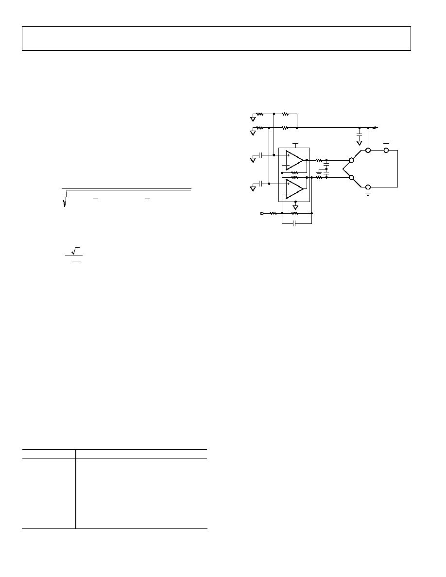
SINGLE-TO-DIFFERENTIAL DRIVER
For applications using a single-ended analog signal, either
bipolar or unipolar, the ADA4941-1 single-ended-to-differential
driver allows for a differential input into the part. The schematic
is shown in Figure 32.
AD7691
REF
GND
VDD
IN+
2.7nF
100nF
2.7nF
IN–
+5V REF
±10V, ±5V, ...
+5.2V
15
10F
15
R2
CF
ADA4941
R1
R3
100nF
R5
R4
R6
06
14
6-
01
0
Figure 32. Single-Ended-to-Differential Driver Circuit
R1 and R2 set the attenuation ratio between the input range and
the ADC range (VREF). R1, R2, and CF are chosen depending on
the desired input resistance, signal bandwidth, antialiasing, and
noise contribution. For example, for the ±10 V range with a 4 kΩ
impedance, R2 = 1 kΩ and R1 = 4 kΩ.
R3 and R4 set the common mode on the IN input, and R5 and
R6 set the common mode on the IN+ input of the ADC. The
common mode should be set close to VREF/2; however, if single
supply is desired, it can be set slightly above VREF/2 to provide
some headroom for the ADA4941-1 output stage. For example,
for the ±10 V range with a single supply, R3 = 8.45 kΩ, R4 =
11.8 kΩ, R5 = 10.5 kΩ, and R6 = 9.76 kΩ.
VOLTAGE REFERENCE INPUT
The AD7691 voltage reference input, REF, has a dynamic input
impedance and should therefore be driven by a low impedance
source with efficient decoupling between the REF and GND
pins, as explained in the Layout section.
When REF is driven by a very low impedance source, for
10 μF (X5R, 0805 size) ceramic chip capacitor is appropriate for
optimum performance.
If an unbuffered reference voltage is used, the decoupling value
depends on the reference used. For instance, a 22 μF (X5R,
1206 size) ceramic chip capacitor is appropriate for optimum
performance using a low temperature drift ADR43x reference.
If desired, smaller reference decoupling capacitor values as low
as 2.2 μF can be used with a minimal impact on performance,
especially DNL.
Regardless, there is no need for an additional lower value
ceramic decoupling capacitor (for example, 100 nF) between the
REF and GND pins.
相关PDF资料 |
PDF描述 |
|---|---|
| STD12W-W | WIRE & CABLE MARKERS |
| REC5-0505SRW/H6/A | CONV DC/DC 5W 4.5-9VIN 05VOUT |
| RCM15DRMN | CONN EDGECARD 30POS .156 WW |
| STD12W-S | WIRE & CABLE MARKERS |
| ADR425ARMZ-REEL7 | IC VREF SERIES PREC 5V 8-MSOP |
相关代理商/技术参数 |
参数描述 |
|---|---|
| EVAL-AD7693CB | 制造商:Analog Devices 功能描述:EVAL KIT FOR 16BIT, 0.5 LSB, 500 KSPS PULSARDIFFERENTIAL ADC - Bulk |
| EVAL-AD7693CBZ | 功能描述:BOARD EVALUATION FOR AD7693 RoHS:是 类别:编程器,开发系统 >> 评估板 - 模数转换器 (ADC) 系列:PulSAR® 产品培训模块:Obsolescence Mitigation Program 标准包装:1 系列:- ADC 的数量:1 位数:12 采样率(每秒):94.4k 数据接口:USB 输入范围:±VREF/2 在以下条件下的电源(标准):- 工作温度:-40°C ~ 85°C 已用 IC / 零件:MAX11645 已供物品:板,软件 |
| EVAL-AD7693SDZ | 功能描述:数据转换 IC 开发工具 EVAL BOARD 16-bit ADC 500kSPS RoHS:否 制造商:Texas Instruments 产品:Demonstration Kits 类型:ADC 工具用于评估:ADS130E08 接口类型:SPI 工作电源电压:- 6 V to + 6 V |
| EVAL-AD7694CB | 制造商:Analog Devices 功能描述: |
| EVAL-AD7694CB1 | 制造商:AD 制造商全称:Analog Devices 功能描述:16-Bit, 250 kSPS PulSAR ADC in MSOP |
发布紧急采购,3分钟左右您将得到回复。