- 您现在的位置:买卖IC网 > PDF目录17031 > EVAL-AD7715-3EBZ (Analog Devices Inc)BOARD EVALUATION FOR AD7715 PDF资料下载
参数资料
| 型号: | EVAL-AD7715-3EBZ |
| 厂商: | Analog Devices Inc |
| 文件页数: | 13/40页 |
| 文件大小: | 0K |
| 描述: | BOARD EVALUATION FOR AD7715 |
| 标准包装: | 1 |
| ADC 的数量: | 1 |
| 位数: | 16 |
| 采样率(每秒): | 500 |
| 数据接口: | 串行 |
| 输入范围: | ±VREF/增益 |
| 在以下条件下的电源(标准): | 5.3mW @ 3.3 V |
| 工作温度: | -40°C ~ 85°C |
| 已用 IC / 零件: | AD7715-3 |
| 已供物品: | 板,CD |
| 相关产品: | AD7715ARUZ-5-ND - IC ADC 16BIT SIGMA-DELTA 16TSSOP AD7715ARUZ-3-ND - IC ADC 16BIT SIGMA-DELTA 16TSSOP AD7715ANZ-3-ND - IC ADC 16BIT SIGMA-DELTA 16DIP AD7715ARUZ-5REEL7-ND - IC ADC 16BIT SIGMA-DELTA 16TSSOP AD7715ARUZ-3REEL7-ND - IC ADC 16BIT SIGMA-DELTA 16TSSOP AD7715ARZ-3REEL-ND - IC ADC 16BIT SIGMA-DELTA 16SOIC AD7715ARZ-3-ND - IC ADC 16BIT 3V 16-SOIC AD7715ANZ-5-ND - IC ADC 16BIT 5V 16-DIP AD7715ARZ-5REEL-ND - IC ADC 16BIT 5V 16-SOIC AD7715ARZ-5-ND - IC ADC 16BIT SIGMA-DELTA 16-SOIC 更多... |
第1页第2页第3页第4页第5页第6页第7页第8页第9页第10页第11页第12页当前第13页第14页第15页第16页第17页第18页第19页第20页第21页第22页第23页第24页第25页第26页第27页第28页第29页第30页第31页第32页第33页第34页第35页第36页第37页第38页第39页第40页
AD7715
Rev. D | Page 20 of 40
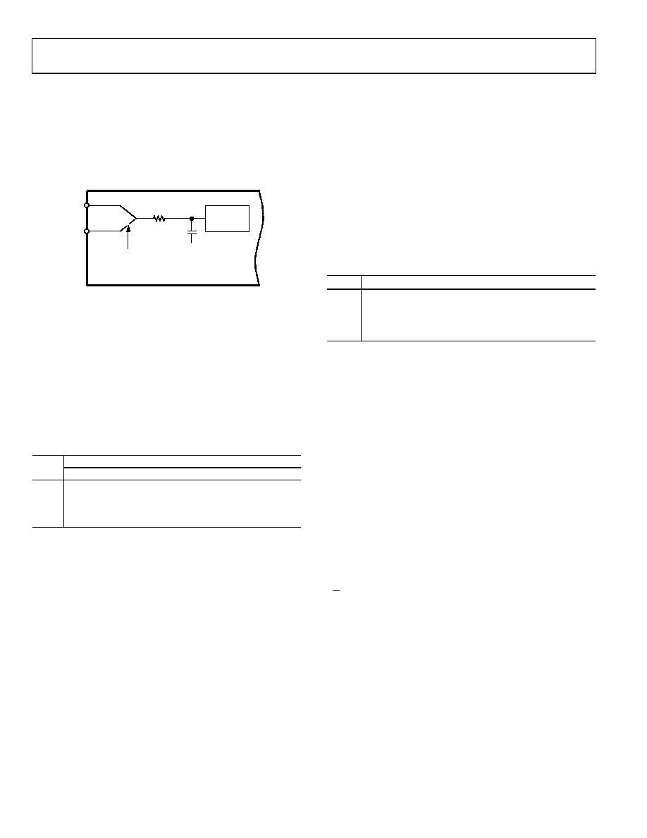
In unbuffered mode, the analog inputs look directly into the
input sampling capacitor, CSAMP. The dc input leakage current in
this unbuffered mode is 1 nA maximum. As a result, the analog
inputs see a dynamic load that is switched at the input sample
rate (see Figure 5). This sample rate depends on master clock
frequency and selected gain. CSAMP is charged to AIN(+) and
discharged to AIN() every input sample cycle. The effective
on-resistance of the switch, RSW, is typically 7 kΩ .
HIGH
IMPEDANCE
>1G
RSW (7k TYP)
CSAMP
(10pF)
VBIAS
SWITCHING FREQUENCY
DEPENDS ON
fCLKIN AND
SELECTED GAIN
AIN(+)
AIN(–)
08
51
9-
00
5
Figure 5. Unbuffered Analog Input Structure
CSAMP must be charged through RSW and through any external
source impedances every input sample cycle. Therefore, in
unbuffered mode, source impedances mean a longer charge
time for CSAMP, and this may result in gain errors on the part.
Table 24 shows the allowable external resistance/capacitance
values, for unbuffered mode, such that no gain error to the
16-bit level is introduced on the part. Note that these capacitances
are total capacitances on the analog input, external capacitance
plus 10 pF capacitance from the pins and lead frame of the device.
Table 24. External R, C Combination for No 16-Bit Gain
Error (Unbuffered Mode Only)
External Capacitance (pF)
Gain
10
50
100
500
1000
5000
1
152 kΩ
53.9 kΩ
31.4 kΩ
8.4 kΩ
4.76 kΩ
1.36 kΩ
2
75.1 kΩ
26.6 kΩ
15.4 kΩ
4.14 kΩ
2.36 kΩ
670 Ω
32
16.7 kΩ
5.95 kΩ
3.46 kΩ
924 Ω
526 Ω
150 Ω
128
16.7 kΩ
5.95 kΩ
3.46 kΩ
924 Ω
526 Ω
150 Ω
In buffered mode, the analog inputs look into the high impedance
inputs stage of the on-chip buffer amplifier. CSAMP is charged via
this buffer amplifier such that source impedances do not affect
the charging of CSAMP. This buffer amplifier has an offset leakage
current of 1 nA. In this buffered mode, large source impedances
result in a small dc offset voltage developed across the source
impedance but not in a gain error.
Input Sample Rate
The modulator sample frequency for the AD7715 remains at
fCLK IN/128 (19.2 kHz @ fCLK IN = 2.4576 MHz) regardless of the
selected gain. However, gains greater than 1 are achieved by a
combination of multiple input samples per modulator cycle and
a scaling of the ratio of reference capacitor to input capacitor. As
a result of the multiple sampling, the input sample rate of the device
varies with the selected gain (see Table 25). In buffered mode, the
input is buffered before the input sampling capacitor. In unbuffered
mode, where the analog input looks directly into the sampling
capacitor, the effective input impedance is 1/CSAMP × fS where
CSAMP is the input sampling capacitance and fS is the input
sample rate.
Table 25. Input Sampling Frequency vs. Gain
Gain
Input Sampling Frequency (fS)
1
fCLK IN/64 (38.4 kHz @ fCLK IN = 2.4576 MHz)
2
2 × fCLK IN/64 (76.8 kHz @ fCLK IN = 2.4576 MHz)
32
8 × fCLK IN/64 (307.2 kHz @ fCLK IN = 2.4576 MHz)
128
8 × fCLK IN/64 (307.2 kHz @ fCLK IN = 2.4576 MHz)
Bipolar/Unipolar Inputs
The analog input on the AD7715 can accept either unipolar or
bipolar input voltage ranges. Bipolar input ranges do not imply
that the part can handle negative voltages on its analog input
since the analog input cannot go more negative than 30 mV to
ensure correct operation of the part. The input channel is fully
differential. As a result, the voltage to which the unipolar and
bipolar signals on the AIN(+) input are referenced is the voltage
on the respective AIN() input. For example, if AIN() is
2.5 V and the AD7715 is configured for unipolar operation with
a gain of 2 and a VREF of 2.5 V, the input voltage range on the
AIN(+) input is 2.5 V to 3.75 V. If AIN() is 2.5 V and the
AD7715 is configured for bipolar mode with a gain of 2 and a
VREF of 2.5 V, the analog input range on the AIN(+) input is
1.25 V to 3.75 V (that is, 2.5 V ± 1.25 V). If AIN() is at AGND,
the part cannot be configured for bipolar ranges in excess of
±30 mV.
Bipolar or unipolar options are chosen by programming the
B/U bit of the setup register. This programs the channel for
either unipolar or bipolar operation. Programming the channel
for either unipolar or bipolar operation does not change any
of the input signal conditioning; it simply changes the data
output coding and the points on the transfer function where
calibrations occur.
相关PDF资料 |
PDF描述 |
|---|---|
| MLG1005S0N3C | INDUCTOR MULTILAYER 0.3NH 0402 |
| DC1500A-C | BOARD SAR ADC LTC2391-16 |
| STD17W-F | WIRE & CABLE MARKERS |
| EVAL-AD7705EBZ | BOARD EVALUATION FOR AD7705 |
| DC1500A-B | BOARD SAR ADC LTC2392-16 |
相关代理商/技术参数 |
参数描述 |
|---|---|
| EVAL-AD7715-3EBZ1 | 制造商:AD 制造商全称:Analog Devices 功能描述:3 V/5 V, 450 ??A 16-Bit, Sigma-Delta ADC |
| EVAL-AD7715-5EB | 制造商:Analog Devices 功能描述:EVLAUATION BOARD - Bulk |
| EVAL-AD7716EB | 制造商:Analog Devices 功能描述:LC2MOS 22-BIT DATA ACQUISITION SYSTEM 制造商:Analog Devices 功能描述:EVALUATION BOARD - Bulk |
| EVAL-AD7716EBZ | 制造商:Analog Devices 功能描述:EVAL BRD AD7716 - Bulk |
| EVAL-AD7718EB | 制造商:Analog Devices 功能描述:Evaluation Kit For 8-/10-Channel, Low Voltage, Low Power, Segma-Delta ADCs 制造商:Rochester Electronics LLC 功能描述:EVALUATION BOARD I.C. - Bulk |
发布紧急采购,3分钟左右您将得到回复。