- 您现在的位置:买卖IC网 > PDF目录17031 > EVAL-AD7715-3EBZ (Analog Devices Inc)BOARD EVALUATION FOR AD7715 PDF资料下载
参数资料
| 型号: | EVAL-AD7715-3EBZ |
| 厂商: | Analog Devices Inc |
| 文件页数: | 21/40页 |
| 文件大小: | 0K |
| 描述: | BOARD EVALUATION FOR AD7715 |
| 标准包装: | 1 |
| ADC 的数量: | 1 |
| 位数: | 16 |
| 采样率(每秒): | 500 |
| 数据接口: | 串行 |
| 输入范围: | ±VREF/增益 |
| 在以下条件下的电源(标准): | 5.3mW @ 3.3 V |
| 工作温度: | -40°C ~ 85°C |
| 已用 IC / 零件: | AD7715-3 |
| 已供物品: | 板,CD |
| 相关产品: | AD7715ARUZ-5-ND - IC ADC 16BIT SIGMA-DELTA 16TSSOP AD7715ARUZ-3-ND - IC ADC 16BIT SIGMA-DELTA 16TSSOP AD7715ANZ-3-ND - IC ADC 16BIT SIGMA-DELTA 16DIP AD7715ARUZ-5REEL7-ND - IC ADC 16BIT SIGMA-DELTA 16TSSOP AD7715ARUZ-3REEL7-ND - IC ADC 16BIT SIGMA-DELTA 16TSSOP AD7715ARZ-3REEL-ND - IC ADC 16BIT SIGMA-DELTA 16SOIC AD7715ARZ-3-ND - IC ADC 16BIT 3V 16-SOIC AD7715ANZ-5-ND - IC ADC 16BIT 5V 16-DIP AD7715ARZ-5REEL-ND - IC ADC 16BIT 5V 16-SOIC AD7715ARZ-5-ND - IC ADC 16BIT SIGMA-DELTA 16-SOIC 更多... |
第1页第2页第3页第4页第5页第6页第7页第8页第9页第10页第11页第12页第13页第14页第15页第16页第17页第18页第19页第20页当前第21页第22页第23页第24页第25页第26页第27页第28页第29页第30页第31页第32页第33页第34页第35页第36页第37页第38页第39页第40页
AD7715
Rev. D | Page 28 of 40
POWER SUPPLIES
There is no specific power sequence required for the AD7715;
either the AVDD or the DVDD supply can come up first. While
the latch-up performance of the AD7715 is good, it is important
that power is applied to the AD7715 before signals at REF IN,
AIN, or the logic input pins to avoid excessive currents. If this
is not possible, then the current that flows in any of these pins
should be limited. If separate supplies are used for the AD7715
and the system digital circuitry, then the AD7715 should be
powered up first. If it is not possible to guarantee this, then
current limiting resistors should be placed in series with the
logic inputs to again limit the current.
During normal operation the AD7715 analog supply (AVDD)
should always be greater than or equal to its digital supply (DVDD).
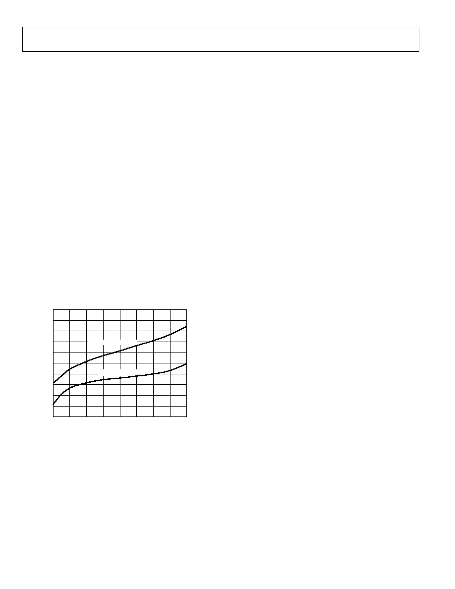
Supply Current
The current consumption on the AD7715 is specified for supplies
in the range 3 V to 3.6 V and in the range 4.75 V to 5.25 V. The
part operates over a 2.85 V to 5.25 V supply range and the IDD
for the part varies as the supply voltage varies over this range.
for both a 1 MHz external clock and a 2.4576 MHz external
clock at 25°C. The AD7715 is operated in unbuffered mode.
The relationship shows that the IDD is minimized by operating
the part with lower VDD voltages. IDD on the AD7715 is also
minimized by using an external master clock or by optimizing
external components when using the on-chip oscillator circuit.
SUPPLY VOLTAGE, AVDD AND DVDD (V)
0
2.85
0.9
1.0
0.8
0.7
0.6
0.5
0.4
0.3
0.2
0.1
3.15
3.45
4.05
4.35
4.65
4.95
5.25
3.75
MCLK IN = 2.4576MHz
MCLK IN = 1MHz
S
UP
P
L
Y
CURR
E
NT
,
A
V
DD
AND
D
V
DD
(m
A
)
08
51
9-
0
07
Figure 7. IDD vs. Supply Voltage
Grounding and Layout
Because the analog inputs and reference input are differential,
most of the voltages in the analog modulator are common-
mode voltages. The excellent common-mode rejection of
the part removes common-mode noise on these inputs. The
analog and digital supplies to the AD7715 are independent
and separately pinned out to minimize coupling between the
analog and digital sections of the device. The digital filter
provides rejection of broadband noise on the power supplies,
except at integer multiples of the modulator sampling
frequency. The digital filter also removes noise from the
analog and reference inputs provided those noise sources do not
saturate the analog modulator. As a result, the AD7715 is more
immune to noise interference than a conventional high
resolution converter. However, because the resolution of the
AD7715 is so high and the noise levels from the AD7715 so low,
care must be taken with regard to grounding and layout.
The printed circuit board that houses the AD7715 should be
designed such that the analog and digital sections are separated
and confined to certain areas of the board. This facilitates the
use of ground planes which can be separated easily. A minimum
etch technique is generally best for ground planes as it gives the
best shielding. Digital and analog ground planes should only be
joined in one place. If the AD7715 is the only device requiring
an AGND to DGND connection, then the ground planes
should be connected at the AGND and DGND pins of the
AD7715. If the AD7715 is in a system where multiple devices
require AGND to DGND connections, the connection should
still be made at one point only, a star ground point which
should be established as close as possible to the AD7715.
Avoid running digital lines under the device as these couples
noise onto the die. The analog ground plane should be allowed
to run under the AD7715 to avoid noise coupling. The power
supply lines to the AD7715 should use as large a trace as
possible to provide low impedance paths and reduce the effects
of glitches on the power supply line. Fast switching signals like
clocks should be shielded with digital ground to avoid radiating
noise to other sections of the board and clock signals should
never be run near the analog inputs. Avoid crossover of digital
and analog signals. Traces on opposite sides of the board should
run at right angles to each other. This reduces the effects of
feedthrough through the board. A microstrip technique is by far
the best but is not always possible with a double-sided board. In
this technique, the component side of the board is dedicated to
ground planes while signals are placed on the solder side.
Good decoupling is important when using high resolution ADCs.
All analog supplies should be decoupled with 10 μF tantalum in
parallel with 0.1 μF capacitors to AGND. To achieve the best
from these decoupling components, they must be placed as close
as possible to the device, ideally right up against the device. All
logic chips should be decoupled with 0.1 μF disc ceramic capacitors
to DGND. In systems where a common supply voltage is used to
drive both the AVDD and DVDD of the AD7715, it is recommended
that the AVDD supply of the system is used. This supply should
have the recommended analog supply decoupling capacitors
between the AVDD pin of the AD7715 and AGND and the
recommended digital supply decoupling capacitor between
the DVDD pin of the AD7715 and DGND.
相关PDF资料 |
PDF描述 |
|---|---|
| MLG1005S0N3C | INDUCTOR MULTILAYER 0.3NH 0402 |
| DC1500A-C | BOARD SAR ADC LTC2391-16 |
| STD17W-F | WIRE & CABLE MARKERS |
| EVAL-AD7705EBZ | BOARD EVALUATION FOR AD7705 |
| DC1500A-B | BOARD SAR ADC LTC2392-16 |
相关代理商/技术参数 |
参数描述 |
|---|---|
| EVAL-AD7715-3EBZ1 | 制造商:AD 制造商全称:Analog Devices 功能描述:3 V/5 V, 450 ??A 16-Bit, Sigma-Delta ADC |
| EVAL-AD7715-5EB | 制造商:Analog Devices 功能描述:EVLAUATION BOARD - Bulk |
| EVAL-AD7716EB | 制造商:Analog Devices 功能描述:LC2MOS 22-BIT DATA ACQUISITION SYSTEM 制造商:Analog Devices 功能描述:EVALUATION BOARD - Bulk |
| EVAL-AD7716EBZ | 制造商:Analog Devices 功能描述:EVAL BRD AD7716 - Bulk |
| EVAL-AD7718EB | 制造商:Analog Devices 功能描述:Evaluation Kit For 8-/10-Channel, Low Voltage, Low Power, Segma-Delta ADCs 制造商:Rochester Electronics LLC 功能描述:EVALUATION BOARD I.C. - Bulk |
发布紧急采购,3分钟左右您将得到回复。