- 您现在的位置:买卖IC网 > PDF目录17051 > EVAL-AD7923CBZ (Analog Devices Inc)BOARD EVAL FOR AD7923 PDF资料下载
参数资料
| 型号: | EVAL-AD7923CBZ |
| 厂商: | Analog Devices Inc |
| 文件页数: | 6/24页 |
| 文件大小: | 0K |
| 描述: | BOARD EVAL FOR AD7923 |
| 标准包装: | 1 |
| ADC 的数量: | 1 |
| 位数: | 12 |
| 采样率(每秒): | 200k |
| 数据接口: | 串行 |
| 输入范围: | 0 ~ 2.5 V |
| 在以下条件下的电源(标准): | 7.5mW @ 200kSPS,5 V |
| 工作温度: | -40°C ~ 125°C |
| 已用 IC / 零件: | AD7923 |
| 已供物品: | 板,CD |
| 相关产品: | AD7923BRUZ-REEL7TR-ND - IC ADC 12BIT 4CH W/SEQ 16TSSOP AD7923BRUZ-REEL-ND - IC ADC 12BIT 4CH W/SEQ 16TSSOP AD7923BRUZ-ND - IC ADC 12BIT 4CH W/SEQ 16TSSOP |
AD7923
Data Sheet
Rev. D | Page 14 of 24
THEORY OF OPERATION
CIRCUIT INFORMATION
The AD7923 is a high speed, 4-channel, 12-bit single-supply
ADC. The part can be operated from a 2.7 V to 5.25 V supply.
When operated from either a 5 V or 3 V supply, the AD7923 is
capable of throughput rates of 200 kSPS. The conversion time
can be as short as 800 ns when provided with a 20 MHz clock.
The AD7923 provides the user with an on-chip track-and-hold
ADC and with a serial interface housed in a 16-lead TSSOP
package. The AD7923 has four, single-ended input channels
with a channel sequencer, allowing the user to select a channel
sequence through which the ADC can cycle with each conse-
utive CS falling edge. The serial clock input accesses data from
the part, controls the transfer of data written to the ADC, and
provides the clock source for the successive approximation
ADC. The analog input range is 0 V to REFIN or 0 V to 2 ×
REFIN, depending on the status of the RANGE bit in the control
register. For the 0 to 2 × REFIN range, the part must be operated
from a 4.75 V to 5.25 V AVDD supply.
The AD7923 provides flexible power management options to
allow the user to achieve the best power performance for a
given throughput rate. These options are selected by program-
ming the power management bits, PM1 and PM0, in the control
register.
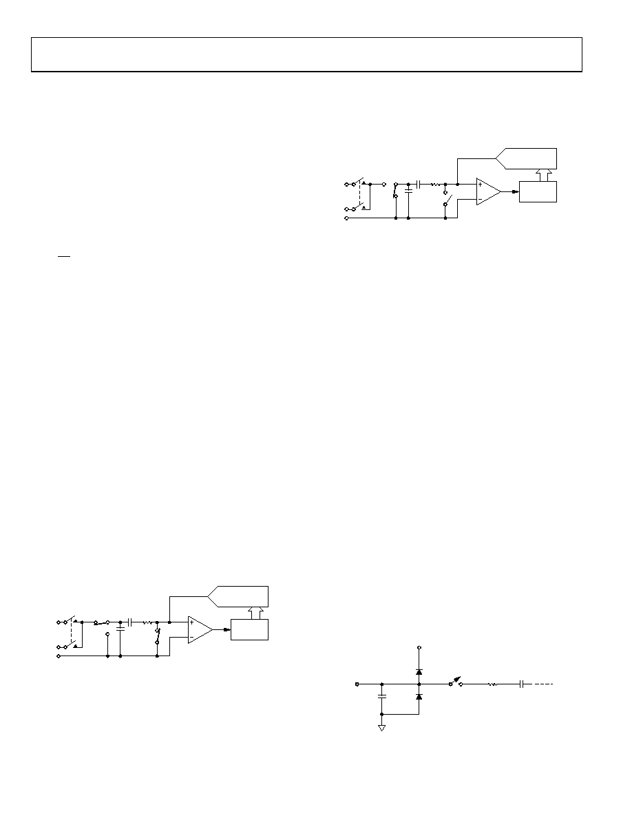
CONVERTER OPERATION
The AD7923 is a 12-bit successive approximation ADC based
around a capacitive DAC. It can convert analog input signals in
Figure 14 show simplified schematics of the ADC. The ADC is
comprised of a control logic, SAR, and capacitive DAC, which
are used to add and subtract fixed amounts of charge from the
sampling capacitor to bring the comparator back into a balanced
condition. Figure 13 shows the ADC during its acquisition phase.
SW2 is closed and SW1 is in Position A. The comparator is held
in a balanced condition and the sampling capacitor acquires the
signal on the selected VIN channel.
VIN0
VIN3
AGND
A
B
SW1
SW2
COMPARATOR
CONTROL
LOGIC
CAPACITIVE
DAC
4k
03086-013
Figure 13. ADC Acquisition Phase
When the ADC starts a conversion (see Figure 14), SW2 opens
and SW1 moves to Position B, causing the comparator to
become unbalanced. The control logic and the capacitive DAC
are used to add and subtract fixed amounts of charge from the
sampling capacitor to bring the comparator back into balance.
When the comparator is rebalanced, the conversion is complete.
The control logic generates the ADC output code. Figure 16 and
Figure 17 show the ADC transfer functions.
VIN0
VIN3
AGND
A
B
SW1
SW2
COMPARATOR
CONTROL
LOGIC
CAPACITIVE
DAC
4k
03086-014
Figure 14. ADC Conversion Phase
Analog Input
Figure 15 shows an equivalent circuit of the analog input
structure of the AD7923. The two diodes D1 and D2 provide
ESD protection for the analog inputs. Care must be taken to
ensure that the analog input signal never exceeds the supply
rails by more than 200 mV; otherwise these diodes become
forward-biased and start conducting current into the substrate.
10 mA is the maximum current these diodes can conduct
without causing irreversible damage to the part. Capacitor C1,
shown in Figure 15, is typically around 4 pF and can primarily
be attributed to pin capacitance. The resistor R1 is a lumped
component made up of the on resistance of the track-and-hold
switch and includes the on resistance of the input multiplexer.
The total resistance is typically about 400 . Capacitor C2 is the
ADC sampling capacitor and has a capacitance of 30 pF typi-
cally. For ac applications, removing high frequency components
from the analog input signal is recommended by using an RC
low-pass filter on the relevant analog input pin. In applications
where harmonic distortion and the signal-to-noise ratio are
critical, the analog input should be driven from a low impe-
dance source. Large source impedances significantly affect the
ac performance of the ADC. This may necessitate the use of an
input buffer amplifier. The choice of the op amp is a function of
the particular application.
When no amplifier is used to drive the analog input, the source
impedance should be limited to low values. The maximum
source impedance depends on the amount of THD that can be
tolerated. The THD increases as the source impedance increases
and performance degrades (see Figure 8).
VIN
C1
4pF
C2
30pF
R1
D1
D2
AVDD
CONVERSION PHASE: SWITCH OPEN
TRACK PHASE: SWITCH CLOSED
03086-015
Figure 15. Equivalent Analog Input Circuit
相关PDF资料 |
PDF描述 |
|---|---|
| AT-S-26-8/8/W-25-OE-R | MOD CORD SGL-ENDED 8-8 WHITE 25' |
| NRS8030T1R0NJGJ | INDUCTOR POWER 1.0UH 6.2A SMD |
| GCC28DCMT | CONN EDGECARD 56POS .100" WW |
| EVAL-AD7899CBZ | BOARD EVAL FOR AD7899 |
| VI-BND-EY | CONVERTER MOD DC/DC 85V 50W |
相关代理商/技术参数 |
参数描述 |
|---|---|
| EVAL-AD7927CB | 制造商:Analog Devices 功能描述:EVALUATION CONTROL BOARD. - Bulk |
| EVAL-AD7927CBZ | 功能描述:BOARD EVALUATION FOR AD7927 RoHS:是 类别:编程器,开发系统 >> 评估板 - 模数转换器 (ADC) 系列:- 产品培训模块:Obsolescence Mitigation Program 标准包装:1 系列:- ADC 的数量:1 位数:12 采样率(每秒):94.4k 数据接口:USB 输入范围:±VREF/2 在以下条件下的电源(标准):- 工作温度:-40°C ~ 85°C 已用 IC / 零件:MAX11645 已供物品:板,软件 |
| EVAL-AD7933CB | 制造商:Analog Devices 功能描述:EVALUATION BOARD 4-CHANNEL, 1.5 MSPS, 10-BIT AND 12-BIT PARALLEL ADCS WITH A SEQUENCER 制造商:Analog Devices 功能描述:EVAL BD FOR 4-CH, 1.5 MSPS, 10-BIT AND 12-BIT PARALLEL ADCS - Bulk |
| EVAL-AD7934-6CB | 制造商:Analog Devices 功能描述:EVAL BD 4-CH, 1.5 MSPS, 10-BIT AND 12-BIT PARALLEL ADCS W/ A - Bulk |
| EVAL-AD7934CB | 制造商:Analog Devices 功能描述:Evaluation Board For 4-Channel, 1.5 MSPS, 10-Bit And 12-Bit Parallel ADCs With A Sequencer 制造商:Analog Devices 功能描述:EVAL BD 4-CH, 1.5 MSPS, 10-BIT AND 12-BIT PARALLEL ADCS W/ A - Bulk |
发布紧急采购,3分钟左右您将得到回复。