- 您现在的位置:买卖IC网 > PDF目录17030 > EVAL-AD974CB (Analog Devices Inc)BOARD EVAL FOR AD974 PDF资料下载
参数资料
| 型号: | EVAL-AD974CB |
| 厂商: | Analog Devices Inc |
| 文件页数: | 16/20页 |
| 文件大小: | 0K |
| 描述: | BOARD EVAL FOR AD974 |
| 标准包装: | 1 |
| ADC 的数量: | 1 |
| 位数: | 16 |
| 采样率(每秒): | 200k |
| 数据接口: | 串行 |
| 输入范围: | ±10 V |
| 在以下条件下的电源(标准): | 120mW @ 200kSPS |
| 工作温度: | -40°C ~ 85°C |
| 已用 IC / 零件: | AD974 |
| 已供物品: | 板 |
| 相关产品: | AD974BRZ-ND - IC DAS 16BIT 4CH 200KSPS 28SOIC AD974BNZ-ND - IC DAS 16BIT 4CH 200KSPS 28DIP AD974ARZ-ND - IC DAS 16BIT 4CH 200KSPS 28-SOIC AD974ARSZ-ND - IC DAS 16BIT 4CH 200KSPS 28-SSOP AD974ANZ-ND - IC DAS 16BIT 4CH 200KSPS 28DIP AD974BRS-RL7-ND - IC DAS 16BIT 4CH 200KSPS 28SSOP AD974BRSZ-ND - IC DAS 16BIT 4CH 200KSPS 28-SSOP AD974BRS-ND - IC DAS 16BIT 4CH 200KSPS 28-SSOP AD974BR-ND - IC DAS 16BIT 4CH 200KSPS 28-SOIC AD974BN-ND - IC DAS 16BIT 4CH 200KSPS 28-DIP 更多... |
REV. A
AD974
–5–
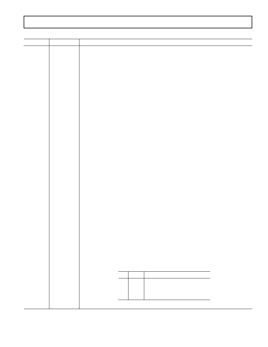
PIN FUNCTION DESCRIPTIONS
Pin No.
Mnemonic
Description
1
AGND1
Analog Ground. Used as the ground reference point for the REF pin.
2–5, 25–28
VxA, VxB
Analog Input. Refer to Table I for input range configuration.
6
BIP
Bipolar Offset. Connect VxA inputs to provide Bipolar input range.
7
CAP
Reference Buffer Output. Connect a 2.2
F tantalum capacitor between CAP and Analog
Ground.
8
REF
Reference Input/Output. The internal +2.5 V reference is available at this pin. Alternatively an
external reference can be used to override the internal reference. In either case, connect a 2.2
F
tantalum capacitor between REF and Analog Ground.
9
AGND2
Analog Ground.
10
R/
C
Read/
Convert Input. Used to control the conversion and read modes. With CS LOW, a falling
edge on R/
C holds the analog input signal internally and starts a conversion; a rising edge enables
the transmission of the conversion result.
11
VDIG
Digital Power Supply. Nominally +5 V.
12
PWRD
Power-Down Input. When set to a logic HIGH, power consumption is reduced and conversions
are inhibited. The conversion result from the previous conversion is stored in the onboard shift
register.
13
EXT/
INT
Digital select input for choosing the internal or an external data clock. With EXT/
INT tied LOW,
after initiating a conversion, 16 DATACLK pulses transmit the previous conversion result as
shown in Figure 3. With EXT/
INT set to a Logic HIGH, output data is synchronized to an
external clock signal connected to the DATACLK input. Data is output as indicated in Figure 4
through Figure 9.
14
DGND
Digital Ground.
15
SYNC
Digital output frame synchronization for use with an external data clock (EXT/
INT = Logic
HIGH). When a read sequence is initiated, a pulse one DATACLK period wide is output
synchronous to the external data clock.
16
DATACLK
Serial data clock input or output, dependent upon the logic state of the EXT/
INT pin. When
using the internal data clock (EXT/
INT = Logic LOW), a conversion start sequence will initiate
transmission of 16 DATACLK periods. Output data is synchronous to this clock and is valid on
both its rising and falling edges (Figure 3). When using an external data clock (EXT/
INT = Logic
HIGH), the
CS and R/C signals control how conversion data is accessed.
17
DATA
The serial data output is synchronized to DATACLK. Conversion results are stored in an on-
chip register. The AD974 provides the conversion result, MSB first, from its internal shift regis-
ter. When using the internal data clock (EXT/
INT = Logic LOW), DATA is valid on both the
rising and falling edges of DATACLK. Using an external data clock (EXT/
INT = Logic HIGH)
allows previous conversion data to be accessed during a conversion (Figures 5, 7 and 9) or the
conversion result can be accessed after the completion of a conversion (Figures 4, 6 and 8).
18, 19
WR1, WR2
Multiplexer Write Inputs. These inputs are internally ORed to generate the mux latch inputs.
The latch is transparent when
WR1 and WR2 are tied low.
20
CS
Chip Select Input. With R/
C LOW, a falling edge on CS will initiate a conversion. With R/C
HIGH, a falling edge on
CS will enable the serial data output sequence.
21
BUSY
Busy Output. Goes LOW when a conversion is started, and remains LOW until the conversion is
completed and the data is latched into the on-chip shift register.
22, 23
A1, A0
Address multiplexer inputs latched with the
WR1, WR2 inputs.
A1
A0
Data Available from Channel
00AIN 1
01AIN 2
10AIN 3
11AIN 4
24
VANA
Analog Power Supply. Nominally +5 V.
相关PDF资料 |
PDF描述 |
|---|---|
| GBM25DCTI | CONN EDGECARD 50POS DIP .156 SLD |
| GCC12DREH-S93 | CONN EDGECARD 24POS .100 EYELET |
| PI5PD2065TAEX | IC POWER DIST USB 2.3A 5SOT23 |
| EYM12DTMS-S189 | CONN EDGECARD 24POS R/A .156 SLD |
| PI5PD2065WEX | IC POWER DIST USB 2.3A 8SOIC |
相关代理商/技术参数 |
参数描述 |
|---|---|
| EVAL-AD976ACB | 功能描述:BOARD EVAL FOR AD976A RoHS:否 类别:编程器,开发系统 >> 评估板 - 模数转换器 (ADC) 系列:- 产品培训模块:Obsolescence Mitigation Program 标准包装:1 系列:- ADC 的数量:1 位数:12 采样率(每秒):94.4k 数据接口:USB 输入范围:±VREF/2 在以下条件下的电源(标准):- 工作温度:-40°C ~ 85°C 已用 IC / 零件:MAX11645 已供物品:板,软件 |
| EVAL-AD976CB | 功能描述:BOARD EVAL FOR AD976 RoHS:否 类别:编程器,开发系统 >> 评估板 - 模数转换器 (ADC) 系列:- 产品培训模块:Obsolescence Mitigation Program 标准包装:1 系列:- ADC 的数量:1 位数:12 采样率(每秒):94.4k 数据接口:USB 输入范围:±VREF/2 在以下条件下的电源(标准):- 工作温度:-40°C ~ 85°C 已用 IC / 零件:MAX11645 已供物品:板,软件 |
| EVAL-AD977ACB | 功能描述:BOARD EVAL FOR AD977A RoHS:否 类别:编程器,开发系统 >> 评估板 - 模数转换器 (ADC) 系列:- 产品培训模块:Obsolescence Mitigation Program 标准包装:1 系列:- ADC 的数量:1 位数:12 采样率(每秒):94.4k 数据接口:USB 输入范围:±VREF/2 在以下条件下的电源(标准):- 工作温度:-40°C ~ 85°C 已用 IC / 零件:MAX11645 已供物品:板,软件 |
| EVAL-AD977CB | 功能描述:BOARD EVAL FOR AD977 RoHS:否 类别:编程器,开发系统 >> 评估板 - 模数转换器 (ADC) 系列:- 产品培训模块:Obsolescence Mitigation Program 标准包装:1 系列:- ADC 的数量:1 位数:12 采样率(每秒):94.4k 数据接口:USB 输入范围:±VREF/2 在以下条件下的电源(标准):- 工作温度:-40°C ~ 85°C 已用 IC / 零件:MAX11645 已供物品:板,软件 |
| EVAL-AD9830EBZ | 功能描述:BOARD EVALUATION AD9830 RoHS:是 类别:编程器,开发系统 >> 评估演示板和套件 系列:- 标准包装:1 系列:- 主要目的:电信,线路接口单元(LIU) 嵌入式:- 已用 IC / 零件:IDT82V2081 主要属性:T1/J1/E1 LIU 次要属性:- 已供物品:板,电源,线缆,CD 其它名称:82EBV2081 |
发布紧急采购,3分钟左右您将得到回复。