- 您现在的位置:买卖IC网 > PDF目录16855 > EVAL-ADF4158EB1Z (Analog Devices Inc)BOARD EVALUATION FOR ADF4158 PDF资料下载
参数资料
| 型号: | EVAL-ADF4158EB1Z |
| 厂商: | Analog Devices Inc |
| 文件页数: | 14/36页 |
| 文件大小: | 0K |
| 描述: | BOARD EVALUATION FOR ADF4158 |
| 标准包装: | 1 |
| 主要目的: | 计时,频率合成器 |
| 嵌入式: | 否 |
| 已用 IC / 零件: | ADF4158 |
| 主要属性: | 单路分数-N PLL |
| 已供物品: | 板 |
第1页第2页第3页第4页第5页第6页第7页第8页第9页第10页第11页第12页第13页当前第14页第15页第16页第17页第18页第19页第20页第21页第22页第23页第24页第25页第26页第27页第28页第29页第30页第31页第32页第33页第34页第35页第36页
Data Sheet
ADF4158
Rev. G | Page 21 of 36
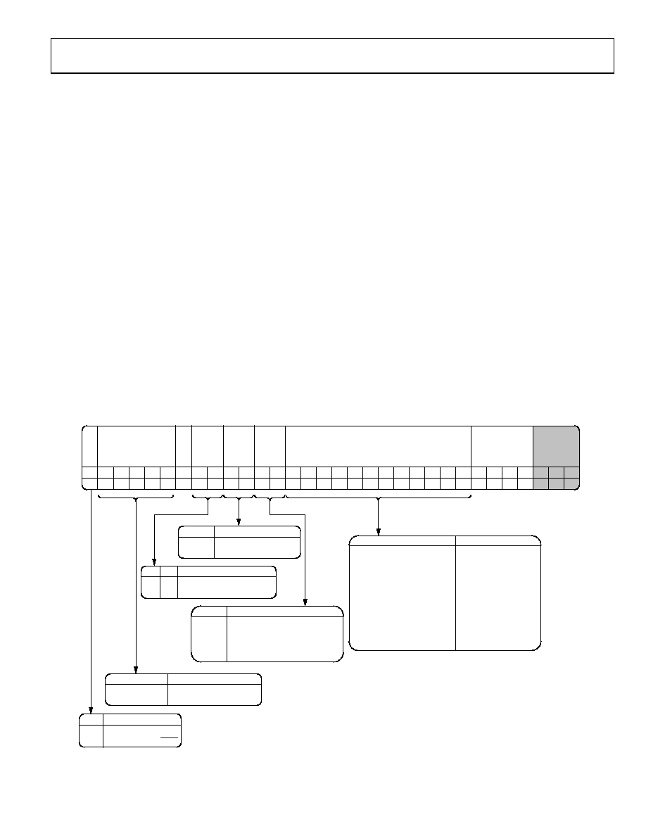
TEST REGISTER (R4) MAP
With Register R4 DB[2:0] set to [1, 0, 0], the on-chip test
register (R4) is programmed as shown in Figure 27.
LE SEL
In some applications, it is necessary to synchronize LE with
the reference signal. To do this, DB31 should be set to 1.
Synchronization is done internally on the part.
Σ-Δ Modulator Mode
To completely disable the Σ-Δ modulator, set Bits DB[30:26] to
0b01110, which puts the ADF4158 into integer-N mode, and
the channel spacing becomes equal to the PFD frequency. Both
the 12-bit MSB fractional value (Register R0, DB[14:3]) and the
13-bit LSB fractional value (Register R1, DB[27:15]) must be set
to 0. After writing to Register 4, Register 3 must be written to twice
to trigger a counter reset. (That is, write Register 3 with DB3 = 1,
and then write Register 3 with DB3 = 0.)
All features driven by the Σ-Δ modulator are disabled, such as
ramping, PSK, FSK, and phase adjust.
Disabling the Σ-Δ modulator also removes the fixed + (fPFD/226)
offset on the VCO output.
For normal operation, set these bits to 0b00000.
Reserved Bits
All reserved bits should be set to 0 for normal operation.
Negative Bleed Current
Setting Bits DB[24:23] to 11 turns on the constant negative
bleed current. This ensures that the charge pump operates out
of the dead zone. Thus, the phase noise is not degraded and the
level of spurs is lower. Enabling constant negative bleed current
is particularly important on channels close to multiple PFD
frequencies. Refer to the AN-1154 Application Note for more
information on the negative bleed current. When using negative
bleed current, readback to MUXOUT must be disabled.
Readback to MUXOUT
DB[22:21] enable or disable the readback to MUXOUT function.
This function allows reading back the synthesizer’s frequency at
the moment of interrupt. When using readback to MUXOUT,
negative bleed current must be off.
Clock Divider (DIV) Mode
Bits DB[20:19] are used to enable ramp divider mode or fast
lock divider mode. If neither is being used, set these bits to 0b00.
12-Bit CLK2 Divider Value
Bits DB[18:7] program the clock divider (the CLK2 timer) when
the part operates in ramp mode (see the Timeout Interval section).
The CLK2 timer also determines how long the loop remains in
wideband mode when fast lock mode is used (see the Fast Lock
Mode section).
DB31
12-BIT CLK2 DIVIDER VALUE
Σ- MODULATOR
MODE
R
ESER
VED
LE
S
E
L
RESERVED
CONTROL
BITS
DB30 DB29 DB28 DB27 DB26 DB25
DB22 DB21 DB20 DB19 DB18 DB17 DB16 DB15 DB14 DB13 DB12 DB11 DB10 DB9 DB8 DB7 DB6 DB5 DB4 DB3 DB2 DB1 DB0
LS1
S5
S4
S3
S2
S1
0
R2R1C2C1
D12
D11 D10
D9D8D7
D6D5D4D3D2
D1
C3(1) C2(0) C1(0)
D12
D11
.......... D2
D1
CLOCK DIVIDER VALUE
0
.
1
0
.
1
0
1
.
0
1
0
1
0
1
.
0
1
0
1
0
1
2
3
.
4092
4093
4094
4095
..........
CK2 CK1 CLOCK DIVIDER MODE
00
CLOCK DIVIDER OFF
01
FAST-LOCK DIVIDER
10
RESERVED
1
RAMP DIVIDER
00
0
CLK
DIV
MODE
READ-
BACK
TO
MUXOUT
08
728
-11
5
DB24 DB23
NB2 NB1
NEG
BLEED
CURR-
ENT
R2
READBACK TO MUXOUT
0
DISABLED
1
ENABLED
R1
0
NB2
NEGATIVE BLEED CURRENT
0OFF
1
ON
NB1
0
1
LS1
LE SEL
0
1
S2
S3
S4
S5
S1
Σ- MODULATOR MODE
0
NORMAL OPERATION
1
0
00
1
010
DISABLED WHEN FRAC = 0
LE FROM PIN
LE SYNCH WITH REFIN
Figure 27. Test Register (R4) Map
相关PDF资料 |
PDF描述 |
|---|---|
| RNF-100-1/8-BK-STK | HEATSHRINK RNF-100 1/8"X4' BLK |
| M3CCA-1418R | IDC CABLE - MKC14A/MC14M/MKC14A |
| M3AAA-1418R | IDC CABLE - MSC14A/MC14M/MSC14A |
| H1AXH-3036G | IDC CABLE - HSC30H/AE30G/X |
| A3AAH-1036G | IDC CABLE - ASC10H/AE10G/ASC10H |
相关代理商/技术参数 |
参数描述 |
|---|---|
| EVAL-ADF4193EBZ1 | 功能描述:BOARD EVALUATION EB1 FOR ADF4193 RoHS:是 类别:编程器,开发系统 >> 评估演示板和套件 系列:- 标准包装:1 系列:- 主要目的:电信,线路接口单元(LIU) 嵌入式:- 已用 IC / 零件:IDT82V2081 主要属性:T1/J1/E1 LIU 次要属性:- 已供物品:板,电源,线缆,CD 其它名称:82EBV2081 |
| EVAL-ADF4193EBZ2 | 功能描述:BOARD EVALUATION EB2 FOR ADF4193 RoHS:是 类别:编程器,开发系统 >> 评估演示板和套件 系列:- 标准包装:1 系列:- 主要目的:电信,线路接口单元(LIU) 嵌入式:- 已用 IC / 零件:IDT82V2081 主要属性:T1/J1/E1 LIU 次要属性:- 已供物品:板,电源,线缆,CD 其它名称:82EBV2081 |
| EVAL-ADF4206-7EB1 | 制造商:Analog Devices 功能描述:EVALUATION BOARD FOR DUAL RF PLL FREQUENCY SYNTHESIZERS 制造商:Analog Devices 功能描述:DUAL RF PLL FREQ SYNTHESIZERS - Bulk |
| EVAL-ADF4208EB1 | 制造商:Analog Devices 功能描述:Evaluation Board For Dual RF PLL Frequency Synthesizers 制造商:Analog Devices 功能描述:DUAL RF PLL FREQ SYNTHESIZERS - Bulk |
| EVAL-ADF4212EB1 | 制造商:Analog Devices 功能描述:EVALUATION BOARD I.C. - Bulk |
发布紧急采购,3分钟左右您将得到回复。