- 您现在的位置:买卖IC网 > PDF目录16855 > EVAL-ADF4158EB1Z (Analog Devices Inc)BOARD EVALUATION FOR ADF4158 PDF资料下载
参数资料
| 型号: | EVAL-ADF4158EB1Z |
| 厂商: | Analog Devices Inc |
| 文件页数: | 4/36页 |
| 文件大小: | 0K |
| 描述: | BOARD EVALUATION FOR ADF4158 |
| 标准包装: | 1 |
| 主要目的: | 计时,频率合成器 |
| 嵌入式: | 否 |
| 已用 IC / 零件: | ADF4158 |
| 主要属性: | 单路分数-N PLL |
| 已供物品: | 板 |
第1页第2页第3页当前第4页第5页第6页第7页第8页第9页第10页第11页第12页第13页第14页第15页第16页第17页第18页第19页第20页第21页第22页第23页第24页第25页第26页第27页第28页第29页第30页第31页第32页第33页第34页第35页第36页
ADF4158
Data Sheet
Rev. G | Page 12 of 36
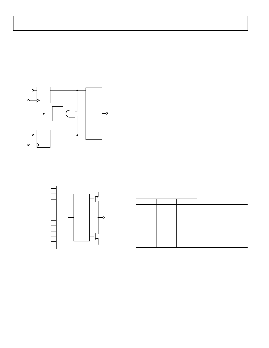
PHASE FREQUENCY DETECTOR (PFD) AND
CHARGE PUMP
The PFD takes inputs from the R-counter and N-counter and
produces an output proportional to the phase and frequency
difference between them. Figure 19 shows a simplified schematic
of the PFD. The PFD includes a fixed delay element that sets the
width of the antibacklash pulse, which is typically 3 ns. This pulse
ensures that there is no dead zone in the PFD transfer function
and gives a consistent reference spur level.
U3
CLR2
Q2
D2
U2
DOWN
UP
HIGH
CP
–IN
+IN
CHARGE
PUMP
DELAY
CLR1
Q1
D1
U1
08
72
8-
0
17
Figure 19. PFD Simplified Schematic
MUXOUT AND LOCK DETECT
The output multiplexer on the ADF4158 allows the user to access
various internal points on the chip. The state of MUXOUT is
controlled by the M4, M3, M2, and M1 bits (see Figure 23).
Figure 20 shows the MUXOUT section in block diagram form.
MUXOUT
DVDD
THREE-STATE OUTPUT
N-DIVIDER OUTPUT
DVDD
DGND
R-DIVIDER OUTPUT
DIGITAL LOCK DETECT
SERIAL DATA OUTPUT
CLK DIVIDER OUTPUT
R-DIVIDER/2
N-DIVIDER/2
FAST-LOCK SWITCH
READBACK TO MUXOUT
CONTROL
MUX
0
872
8-
0
09
Figure 20. MUXOUT Schematic
INPUT SHIFT REGISTERS
The ADF4158 digital section includes a 5-bit RF R-counter, a
12-bit RF N-counter, and a 25-bit FRAC counter. Data is clocked
into the 32-bit shift register on each rising edge of CLK. The
data is clocked in MSB first. Data is transferred from the shift
register to one of eight latches on the rising edge of LE. The
destination latch is determined by the state of the three control
bits (C3, C2, and C1) in the shift register. These are the three
LSBs—DB2, DB1, and DB0—as shown in Figure 2. The truth
show a summary of how the latches are programmed.
PROGRAM MODES
program modes in the ADF4158.
Several settings in the ADF4158 are double buffered. These include
the LSB fractional value, R-counter value, reference doubler,
current setting, and RDIV2. This means that two events must
occur before the part uses a new value for any of the double-
buffered settings. First, the new value is latched into the device
by writing to the appropriate register. Second, a new write must
be performed on Register R0.
For example, updating the fractional value can involve a write to
the 13 LSB bits in R1 and the 12 MSB bits in R0. R1 should be
written to first, followed by the write to R0. The frequency change
begins after the write to R0. Double buffering ensures that the
bits written to in R1 do not take effect until after the write to R0.
Table 6. C3, C2, and C1 Truth Table
Control Bits
C3
C2
C1
Register
0
R0
0
1
R1
0
1
0
R2
0
1
R3
1
0
R4
1
0
1
R5
1
0
R6
1
R7
相关PDF资料 |
PDF描述 |
|---|---|
| RNF-100-1/8-BK-STK | HEATSHRINK RNF-100 1/8"X4' BLK |
| M3CCA-1418R | IDC CABLE - MKC14A/MC14M/MKC14A |
| M3AAA-1418R | IDC CABLE - MSC14A/MC14M/MSC14A |
| H1AXH-3036G | IDC CABLE - HSC30H/AE30G/X |
| A3AAH-1036G | IDC CABLE - ASC10H/AE10G/ASC10H |
相关代理商/技术参数 |
参数描述 |
|---|---|
| EVAL-ADF4193EBZ1 | 功能描述:BOARD EVALUATION EB1 FOR ADF4193 RoHS:是 类别:编程器,开发系统 >> 评估演示板和套件 系列:- 标准包装:1 系列:- 主要目的:电信,线路接口单元(LIU) 嵌入式:- 已用 IC / 零件:IDT82V2081 主要属性:T1/J1/E1 LIU 次要属性:- 已供物品:板,电源,线缆,CD 其它名称:82EBV2081 |
| EVAL-ADF4193EBZ2 | 功能描述:BOARD EVALUATION EB2 FOR ADF4193 RoHS:是 类别:编程器,开发系统 >> 评估演示板和套件 系列:- 标准包装:1 系列:- 主要目的:电信,线路接口单元(LIU) 嵌入式:- 已用 IC / 零件:IDT82V2081 主要属性:T1/J1/E1 LIU 次要属性:- 已供物品:板,电源,线缆,CD 其它名称:82EBV2081 |
| EVAL-ADF4206-7EB1 | 制造商:Analog Devices 功能描述:EVALUATION BOARD FOR DUAL RF PLL FREQUENCY SYNTHESIZERS 制造商:Analog Devices 功能描述:DUAL RF PLL FREQ SYNTHESIZERS - Bulk |
| EVAL-ADF4208EB1 | 制造商:Analog Devices 功能描述:Evaluation Board For Dual RF PLL Frequency Synthesizers 制造商:Analog Devices 功能描述:DUAL RF PLL FREQ SYNTHESIZERS - Bulk |
| EVAL-ADF4212EB1 | 制造商:Analog Devices 功能描述:EVALUATION BOARD I.C. - Bulk |
发布紧急采购,3分钟左右您将得到回复。