- 您现在的位置:买卖IC网 > Datasheet目录415 > FDC6310P (Fairchild Semiconductor)MOSFET P-CH DUAL 20V SSOT-6 Datasheet资料下载
参数资料
| 型号: | FDC6310P |
| 厂商: | Fairchild Semiconductor |
| 文件页数: | 1/5页 |
| 文件大小: | 0K |
| 描述: | MOSFET P-CH DUAL 20V SSOT-6 |
| 产品培训模块: | High Voltage Switches for Power Processing |
| 产品变化通告: | Mold Compound Change 08/April/2008 |
| 标准包装: | 1 |
| 系列: | PowerTrench® |
| FET 型: | 2 个 P 沟道(双) |
| FET 特点: | 逻辑电平门 |
| 漏极至源极电压(Vdss): | 20V |
| 电流 - 连续漏极(Id) @ 25° C: | 2.2A |
| 开态Rds(最大)@ Id, Vgs @ 25° C: | 125 毫欧 @ 2.2A,4.5V |
| Id 时的 Vgs(th)(最大): | 1.5V @ 250µA |
| 闸电荷(Qg) @ Vgs: | 5.2nC @ 4.5V |
| 输入电容 (Ciss) @ Vds: | 337pF @ 10V |
| 功率 - 最大: | 700mW |
| 安装类型: | 表面贴装 |
| 封装/外壳: | SOT-23-6 细型,TSOT-23-6 |
| 供应商设备封装: | 6-SSOT |
| 包装: | 标准包装 |
| 其它名称: | FDC6310PFSDKR |
�� �
�
�April� 2001�
�FDC6310P�
�Dual� P-Channel� 2.5V� Specified� PowerTrench� ?� MOSFET�
�General� Description�
�These� P-Channel� 2.5V� specified� MOSFETs� are�
�produced� using� Fairchild� Semiconductor's� advanced�
�PowerTrench� process� that� has� been� especially� tailored�
�to� minimize� on-state� resistance� and� yet� maintain� low�
�gate� charge� for� superior� switching� performance.�
�These� devices� have� been� designed� to� offer� exceptional�
�power� dissipation� in� a� very� small� footprint� for�
�applications� where� the� bigger� more� expensive� SO-8�
�and� TSSOP-8� packages� are� impractical.�
�Applications�
�?� Load� switch�
�?� Battery� protection�
�?� Power� management�
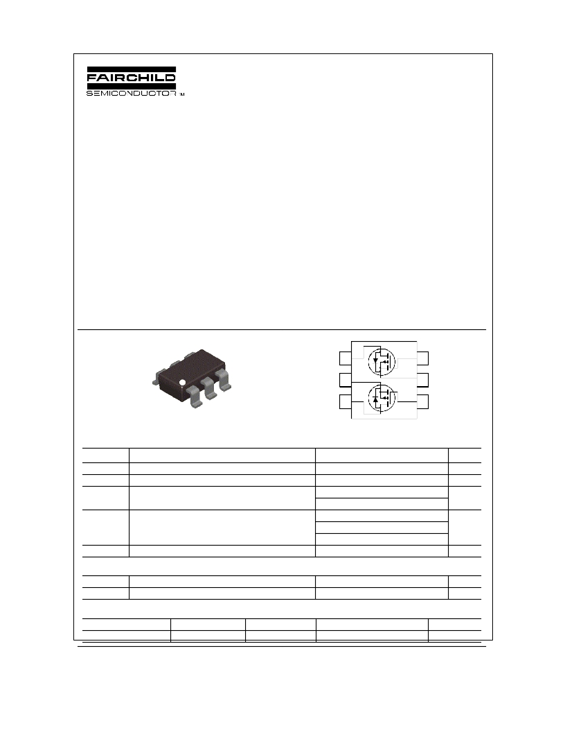
�D2�
�Features�
�?� –2.2� A,� –20� V.� R� DS(ON)� =� 125� m� ?� @� V� GS� =� –4.5� V�
�R� DS(ON)� =� 190� m� ?� @� V� GS� =� –2.5� V�
�?� Low� gate� charge�
�?� Fast� switching� speed�
�?� High� performance� trench� technology� for� extremely�
�low� R� DS(ON)�
�?� SuperSOT� TM� -6� package:� small� footprint� 72%�
�smaller� than� standard� SO-8);� low� profile� (1mm� thick)�
�D1�
�S1�
�4�
�5�
�3�
�2�
�SuperSOT�
�TM�
�-6�
�G1�
�S2�
�G2�
�6�
�1�
�Absolute� Maximum� Ratings�
�T� A� =25� o� C� unless� otherwise� noted�
�Symbol�
�V� DSS�
�V� GSS�
�Parameter�
�Drain-Source� Voltage�
�Gate-Source� Voltage�
�Ratings�
�–20�
�±� 12�
�Units�
�V�
�V�
�I� D�
�Drain� Current�
�–� Continuous�
�(Note� 1a)�
�–2.2�
�A�
�–� Pulsed�
�–6�
�P� D�
�Power� Dissipation� for� Single� Operation�
�(Note� 1a)�
�0.96�
�W�
�(Note� 1b)�
�(Note� 1c)�
�0.9�
�0.7�
�T� J� ,� T� STG�
�Operating� and� Storage� Junction� Temperature� Range�
�–55� to� +150�
�°� C�
�Thermal� Characteristics�
�R� θ� JA�
�R� θ� J� C�
�Thermal� Resistance,� Junction-to-Ambient�
�Thermal� Resistance,� Junction-to-Case�
�(Note� 1a)�
�(Note� 1)�
�130�
�60�
�°� C/W�
�°� C/W�
�Package� Marking� and� Ordering� Information�
�Device� Marking�
�.310�
�Device�
�FDC6310P�
�Reel� Size�
�7’’�
�Tape� width�
�8mm�
�Quantity�
�3000� units�
�?� 2001� Fairchild� Semiconductor� Corporation�
�FDC6310P� Rev� C(W)�
�相关PDF资料 |
PDF描述 |
|---|---|
| FDC6312P | MOSFET P-CH DUAL 20V SSOT-6 |
| FDC6318P | MOSFET P-CH DUAL 12V SSOT-6 |
| FDC6320C | MOSFET N/P-CH DUAL 25V SSOT6 |
| FDC6321C | MOSFET N/P-CH DUAL 25V SSOT-6 |
| FDC6327C | MOSFET N/P-CH DUAL 20V SSOT-6 |
相关代理商/技术参数 |
参数描述 |
|---|---|
| FDC6310P_Q | 功能描述:MOSFET Dual P-Ch 2.5V Spec Power Trench RoHS:否 制造商:STMicroelectronics 晶体管极性:N-Channel 汲极/源极击穿电压:650 V 闸/源击穿电压:25 V 漏极连续电流:130 A 电阻汲极/源极 RDS(导通):0.014 Ohms 配置:Single 最大工作温度: 安装风格:Through Hole 封装 / 箱体:Max247 封装:Tube |
| FDC6312P | 功能描述:MOSFET SSOT-6 P-CH DUAL RoHS:否 制造商:STMicroelectronics 晶体管极性:N-Channel 汲极/源极击穿电压:650 V 闸/源击穿电压:25 V 漏极连续电流:130 A 电阻汲极/源极 RDS(导通):0.014 Ohms 配置:Single 最大工作温度: 安装风格:Through Hole 封装 / 箱体:Max247 封装:Tube |
| FDC6312P | 制造商:Fairchild Semiconductor Corporation 功能描述:MOSFET |
| FDC6312P_Q | 功能描述:MOSFET SSOT-6 P-CH DUAL RoHS:否 制造商:STMicroelectronics 晶体管极性:N-Channel 汲极/源极击穿电压:650 V 闸/源击穿电压:25 V 漏极连续电流:130 A 电阻汲极/源极 RDS(导通):0.014 Ohms 配置:Single 最大工作温度: 安装风格:Through Hole 封装 / 箱体:Max247 封装:Tube |
| FDC6318 | 制造商:FAIRCHILD 制造商全称:Fairchild Semiconductor 功能描述:Dual P-Channel 1.8V PowerTrench Specified MOSFET |
发布紧急采购,3分钟左右您将得到回复。