- 您现在的位置:买卖IC网 > Datasheet目录424 > FDP2572 (Fairchild Semiconductor)MOSFET N-CH 150V 29A TO-220AB Datasheet资料下载
参数资料
| 型号: | FDP2572 |
| 厂商: | Fairchild Semiconductor |
| 文件页数: | 2/11页 |
| 文件大小: | 0K |
| 描述: | MOSFET N-CH 150V 29A TO-220AB |
| 产品培训模块: | High Voltage Switches for Power Processing |
| 标准包装: | 400 |
| 系列: | PowerTrench® |
| FET 型: | MOSFET N 通道,金属氧化物 |
| FET 特点: | 标准 |
| 漏极至源极电压(Vdss): | 150V |
| 电流 - 连续漏极(Id) @ 25° C: | 29A |
| 开态Rds(最大)@ Id, Vgs @ 25° C: | 54 毫欧 @ 9A,10V |
| Id 时的 Vgs(th)(最大): | 4V @ 250µA |
| 闸电荷(Qg) @ Vgs: | 34nC @ 10V |
| 输入电容 (Ciss) @ Vds: | 1770pF @ 25V |
| 功率 - 最大: | 135W |
| 安装类型: | 通孔 |
| 封装/外壳: | TO-220-3 |
| 供应商设备封装: | TO-220AB |
| 包装: | 管件 |
| 其它名称: | FDP2572-ND FDP2572FS Q1965920 |
�� �
�
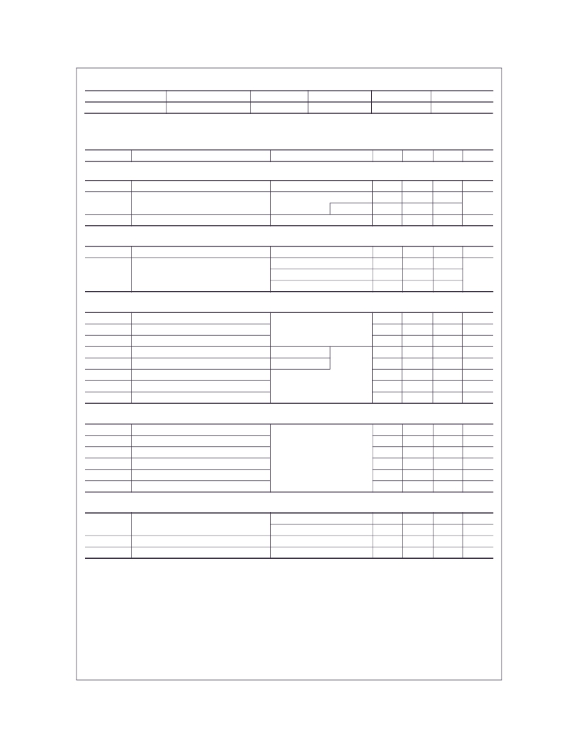
�Package� Marking� and� Ordering� Information�
�Device� Marking�
�FDB2572�
�Device�
�FDB2572�
�Package�
�TO-263AB�
�Reel� Size�
�330mm�
�Tape� Width�
�24mm�
�Quantity�
�800� units�
�Electrical� Characteristics� T� C� =� 25°C� unless� otherwise� noted�
�Symbol�
�Parameter�
�Test� Conditions�
�Min�
�Typ�
�Max�
�Units�
�Off� Characteristics�
�B� VDSS�
�Drain� to� Source� Breakdown� Voltage�
�I� D� =� 250� μ� A,� V� GS� =� 0V�
�150�
�-�
�-�
�V�
�I� DSS�
�I� GSS�
�Zero� Gate� Voltage� Drain� Current�
�Gate� to� Source� Leakage� Current�
�V� DS� =� 120V�
�V� GS� =� 0V�
�V� GS� =� ±� 20V�
�T� C� =� 150� o�
�-�
�-�
�-�
�-�
�-�
�-�
�1�
�250�
�±� 100�
�μ� A�
�nA�
�On� Characteristics�
�V� GS(TH)�
�Gate� to� Source� Threshold� Voltage�
�V� GS� =� V� DS� ,� I� D� =� 250� μ� A�
�2�
�-�
�4�
�V�
�I� D� =9A,� V� GS� =10V�
�-�
�0.045�
�0.054�
�r� DS(ON)�
�Drain� to� Source� On� Resistance�
�I� D� =� 4A,� V� GS� =� 6V,�
�-�
�0.050�
�0.075�
�?�
�I� D� =9A,� V� GS� =10V,� T� C� =175� o� C�
�-�
�0.126�
�0.146�
�Dynamic� Characteristics�
�C� ISS�
�C� OSS�
�C� RSS�
�Q� g(TOT)�
�Input� Capacitance�
�Output� Capacitance�
�Reverse� Transfer� Capacitance�
�Total� Gate� Charge� at� 10V�
�V� DS� =� 25V,� V� GS� =� 0V,�
�f� =� 1MHz�
�V� GS� =� 0V� to� 10V�
�-�
�-�
�-�
�-�
�1770�
�183�
�40�
�26�
�-�
�-�
�-�
�34�
�pF�
�pF�
�pF�
�nC�
�Q� g(TH)�
�Q� gs�
�Q� gs2�
�Q� gd�
�Threshold� Gate� Charge�
�Gate� to� Source� Gate� Charge�
�Gate� Charge� Threshold� to� Plateau�
�Gate� to� Drain� “Miller”� Charge�
�V� GS� =� 0V� to� 2V�
�V� DD� =� 75V�
�I� D� =� 9A�
�I� g� =� 1.0mA�
�-�
�-�
�-�
�-�
�3.3�
�8�
�5�
�6�
�4.3�
�-�
�-�
�-�
�nC�
�nC�
�nC�
�nC�
�Resistive� Switching� Characteristics� (V� GS� =� 10V)�
�t� ON�
�t� d(ON)�
�Turn-On� Time�
�Turn-On� Delay� Time�
�-�
�-�
�-�
�11�
�36�
�-�
�ns�
�ns�
�t� r�
�t� d(OFF)�
�t� f�
�t� OFF�
�Rise� Time�
�Turn-Off� Delay� Time�
�Fall� Time�
�Turn-Off� Time�
�V� DD� =� 75V,� I� D� =� 9A�
�V� GS� =� 10V,� R� GS� =� 11.0� ?�
�-�
�-�
�-�
�-�
�14�
�31�
�14�
�-�
�-�
�-�
�-�
�66�
�ns�
�ns�
�ns�
�ns�
�Drain-Source� Diode� Characteristics�
�V� SD�
�t� rr�
�Q� RR�
�Source� to� Drain� Diode� Voltage�
�Reverse� Recovery� Time�
�Reverse� Recovered� Charge�
�I� SD� =� 9A�
�I� SD� =� 4A�
�I� SD� =� 9A,� dI� SD� /dt� =100A/� μ� s�
�I� SD� =� 9A,� dI� SD� /dt� =100A/� μ� s�
�-�
�-�
�-�
�-�
�-�
�-�
�-�
�-�
�1.25�
�1.0�
�74�
�169�
�V�
�V�
�ns�
�nC�
�Notes:�
�1:� Starting� T� J� =� 25°C,� L� =� 0.2mH,� I� AS� =� 19A.�
�2:� Pulse� Width� =� 100s�
�?2012� Fairchild� Semiconductor� Corporation�
�FDB2572� Rev.� C�
�相关PDF资料 |
PDF描述 |
|---|---|
| FDP2614 | MOSFET N-CH 200V 62A TO-220 |
| FDP26N40 | MOSFET N-CH 400V 26A TO-220 |
| FDP2710 | MOSFET N-CH 250V 50A TO-220 |
| FDP33N25 | MOSFET N-CH 250V 33A TO-220 |
| FDP3651U | MOSFET N-CH 100V 80A TO-220AB |
相关代理商/技术参数 |
参数描述 |
|---|---|
| FDP2572 | 制造商:Fairchild Semiconductor Corporation 功能描述:MOSFET 制造商:Fairchild Semiconductor Corporation 功能描述:N CH MOSFET, 150V, 29A, TO-220AB |
| FDP2572_12 | 制造商:FAIRCHILD 制造商全称:Fairchild Semiconductor 功能描述:N-Channel PowerTrench?? MOSFET 150V, 29A, 54m?? |
| FDP2572_Q | 功能描述:MOSFET TO-220 N-CH 150V 29A RoHS:否 制造商:STMicroelectronics 晶体管极性:N-Channel 汲极/源极击穿电压:650 V 闸/源击穿电压:25 V 漏极连续电流:130 A 电阻汲极/源极 RDS(导通):0.014 Ohms 配置:Single 最大工作温度: 安装风格:Through Hole 封装 / 箱体:Max247 封装:Tube |
| FDP2614 | 功能描述:MOSFET 200V N-Channel PowerTrench RoHS:否 制造商:STMicroelectronics 晶体管极性:N-Channel 汲极/源极击穿电压:650 V 闸/源击穿电压:25 V 漏极连续电流:130 A 电阻汲极/源极 RDS(导通):0.014 Ohms 配置:Single 最大工作温度: 安装风格:Through Hole 封装 / 箱体:Max247 封装:Tube |
| FDP2670 | 功能描述:MOSFET 200V NCh PowerTrench RoHS:否 制造商:STMicroelectronics 晶体管极性:N-Channel 汲极/源极击穿电压:650 V 闸/源击穿电压:25 V 漏极连续电流:130 A 电阻汲极/源极 RDS(导通):0.014 Ohms 配置:Single 最大工作温度: 安装风格:Through Hole 封装 / 箱体:Max247 封装:Tube |
发布紧急采购,3分钟左右您将得到回复。