- 您现在的位置:买卖IC网 > PDF目录375788 > FDZ7064AS (FAIRCHILD SEMICONDUCTOR CORP) 30V N-Channel PowerTrench SyncFET BGA MOSFET PDF资料下载
参数资料
| 型号: | FDZ7064AS |
| 厂商: | FAIRCHILD SEMICONDUCTOR CORP |
| 元件分类: | JFETs |
| 英文描述: | 30V N-Channel PowerTrench SyncFET BGA MOSFET |
| 中文描述: | 13.5 A, 30 V, 0.0056 ohm, N-CHANNEL, Si, POWER, MOSFET |
| 封装: | ULTRA THIN, 3.50 X 4 MM, 0.76 MM HEIGHT, BGA-30 |
| 文件页数: | 2/7页 |
| 文件大小: | 599K |
| 代理商: | FDZ7064AS |
2
www.fairchildsemi.com
FDZ7064AS Rev. A
F
Electrical Characteristics
T
A
= 25C unless otherwise noted
Notes:
1.
R
side of the solder ball, R
guaranteed by design while R
is determined with the device mounted on a 1 in
, is defined for reference. For R
2
2 oz. copper pad on a 1.5 x 1.5 in. board of FR-4 material. The thermal resistance from the junction to the circuit board
, the thermal reference point for the case is defined as the top surface of the copper chip carrier. R
is determined by the user's board design.
JB
JC
θ
JC
and R
θ
JB
are
θ
JA
2.
Pulse Test: Pulse Width < 300
μ
s, Duty Cycle < 2.0%
Symbol
Parameter
Test Conditions
Min
Typ
Max
Units
Off Characteristics
BV
DSS
BV
T
Drain–Source Breakdown Voltage
V
GS
= 10mA, Referenced to 25
= 0 V, I
D
= 1mA
30
V
DSS
J
Breakdown Voltage Temperature Coefficient I
D
°
C
25
mV/
°
C
I
DSS
Zero Gate Voltage Drain Current
V
DS
= 24 V, V
GS
= 0 V
500
uA
I
GSS
On Characteristics
Gate–Body Leakage
V
GS
= ±20 V, V
DS
= 0 V
±100
nA
(Note 2)
V
GS(th)
V
GS(th)
T
Gate Threshold Voltage
V
DS
= 10mA, Referenced to 25
= V
GS
, I
D
= 1mA
1
1.4
3
V
J
Gate Threshold Voltage
Temperature Coefficient
I
D
°
C
–0.3
mV/
°
C
R
DS(on)
Static Drain–Source
On–Resistance
V
V
V
GS
GS
GS
= 10 V, I
= 4.5 V, I
=10 V, I
D
D
=13.5A, T
= 13.5 A
= 12 A
D
J
=125
°
C
4.6
5.7
5.9
5.6
7.1
7.4
m
I
D(on)
g
FS
Dynamic Characteristics
On–State Drain Current
V
GS
= 10 V,V
DS
= 13.5 A
= 5 V
60
A
Forward Transconductance
V
DS
= 5 V, I
D
61
S
C
iss
Input Capacitance
V
f = 1.0 MHz
DS
= 15 V, V
GS
= 0 V,
1960
pF
C
oss
Output Capacitance
570
pF
C
rss
Reverse Transfer Capacitance
210
pF
R
G
Gate Resistance
V
GS
= 15 mV, I
D
= 6 A
1.4
W
Switching Characteristics
(Note 2)
t
d(on)
Turn–On Delay Time
V
V
DS
GS
= 15 V, I
= 10 V, R
D
= 1 A,
GEN
= 6
9
18
nS
t
r
Turn–On Rise Time
12
22
nS
t
d(off)
Turn–Off Delay Time
39
62
nS
t
f
Turn–Off Fall Time
18
33
nS
Q
g(TOT)
Total Gate Charge, Vgs = 10V
V
DS
= 15 V, I
D
= 13.5A
36
51
nC
Q
g
Total Gate Charge, Vgs = 5V
20
28
nC
Q
gs
Gate–Source Charge
5
nC
Q
gd
Gate–Drain Charge
6
nC
Drain–Source Diode Characteristics
V
SD
Drain–Source Diode Forward Voltage
V
GS
= 13.5 A, d
See Diode Characteristic, page 5
= 0 V, I
S
= 3.2 A (Note 1)
0.4
0.7
V
t
rr
Diode Reverse Recovery Time
I
F
iF
/d
t
= 300 A/μs
23
nS
Q
rr
Diode Reverse Recovery Charge
21
nC
a) 56C/W when mounted on a
1in
pad of 2 oz copper
b) 119C/W when mounted on a mini-
mum pad of 2 oz copper
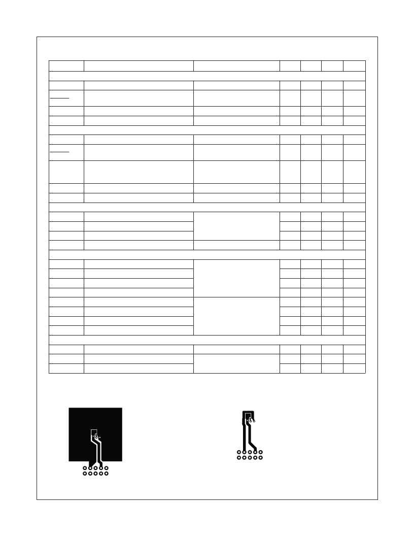
Scale 1 : 1 on letter size paper
相关PDF资料 |
PDF描述 |
|---|---|
| FDZ7064N | 30V N-Channel Logic Level PowerTrench BGA MOSFET |
| FDZ7064S | TERMINAL |
| FDZ7296 | 30V N-Channel PowerTrench BGA MOSFET |
| FE3C | GLASS PASSIVATED FAST EFFICIENT RECTIFIER |
| FE5A | Glass Passivated Fast Efficient Rectifier(钝化玻璃快速效应整流器) |
相关代理商/技术参数 |
参数描述 |
|---|---|
| FDZ7064N | 功能描述:MOSFET 30V N-Ch BGa MOSFET Logic Level RoHS:否 制造商:STMicroelectronics 晶体管极性:N-Channel 汲极/源极击穿电压:650 V 闸/源击穿电压:25 V 漏极连续电流:130 A 电阻汲极/源极 RDS(导通):0.014 Ohms 配置:Single 最大工作温度: 安装风格:Through Hole 封装 / 箱体:Max247 封装:Tube |
| FDZ7064N_Q | 功能描述:MOSFET 30V N-Ch BGa MOSFET Logic Level RoHS:否 制造商:STMicroelectronics 晶体管极性:N-Channel 汲极/源极击穿电压:650 V 闸/源击穿电压:25 V 漏极连续电流:130 A 电阻汲极/源极 RDS(导通):0.014 Ohms 配置:Single 最大工作温度: 安装风格:Through Hole 封装 / 箱体:Max247 封装:Tube |
| FDZ7064S | 功能描述:MOSFET 30V/12V NCh SYNCFET RoHS:否 制造商:STMicroelectronics 晶体管极性:N-Channel 汲极/源极击穿电压:650 V 闸/源击穿电压:25 V 漏极连续电流:130 A 电阻汲极/源极 RDS(导通):0.014 Ohms 配置:Single 最大工作温度: 安装风格:Through Hole 封装 / 箱体:Max247 封装:Tube |
| FDZ7296 | 功能描述:MOSFET 30V N-Ch PowerTrench BGA MOSFET RoHS:否 制造商:STMicroelectronics 晶体管极性:N-Channel 汲极/源极击穿电压:650 V 闸/源击穿电压:25 V 漏极连续电流:130 A 电阻汲极/源极 RDS(导通):0.014 Ohms 配置:Single 最大工作温度: 安装风格:Through Hole 封装 / 箱体:Max247 封装:Tube |
| FDZX2-S4/4 | 制造商:Cooper Bussmann 功能描述:ADAPTR KIT FOR FD800 制造商:COOPER BUSSMANN 功能描述:ADAPTER KIT FOR FD800 |
发布紧急采购,3分钟左右您将得到回复。