- 您现在的位置:买卖IC网 > PDF目录296013 > FM25C041ULZEM8 SPI Serial EEPROM PDF资料下载
参数资料
| 型号: | FM25C041ULZEM8 |
| 英文描述: | SPI Serial EEPROM |
| 中文描述: | SPI串行EEPROM |
| 文件页数: | 10/11页 |
| 文件大小: | 101K |
| 代理商: | FM25C041ULZEM8 |
8
www.fairchildsemi.com
FM25C041U
FM25C041U
4K-Bit
SPI
Interface
Serial
CMOS
EEPROM
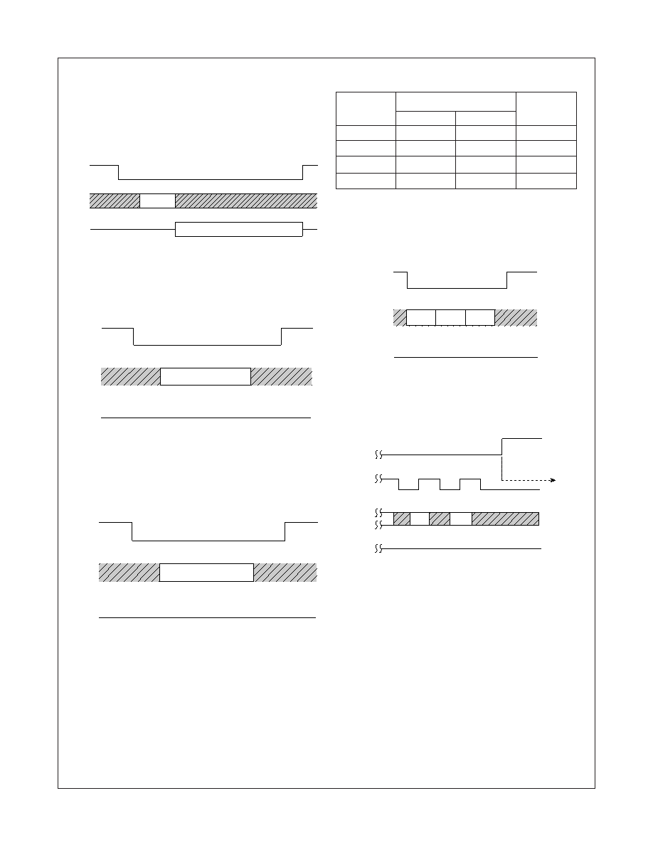
The RDSR command requires the following sequence. The /CS
pin is pulled low to select the EEPROM and then the RDSR
opcode is transmitted on the SI pin. After this is done, data on the
SI pin becomes don’t care. The data from the Status Register is
then shifted out on the SO pin starting with D7 bit first and D0 last.
See
Figure 6.
FIGURE 6. Read Status Register
TABLE 4. Block Write Protection Levels
Level
Status Register Bits
Array
Address
BP1
BP0
Protected
0
None
1
0
1
180-1FF
2
1
0
100-1FF
3
1
000-1FF
A WRITE command requires the following sequence. The /CS pin
is pulled low to select the EEPROM, then the WRITE opcode is
transmitted on the SI pin followed by the byte address (A7-A0) and
followed by the data (D7-D0) to be written. See
Figure 9.
FIGURE 9. Byte Write
/CS
SI
SO
RDSR
OP-CODE
RDSR DATA
WRITE ENABLE (WREN):
When V
CC is applied to the EEPROM, it “powers up” in a write-
disabled state. Therefore, all programming modes (Write to memory
array and Status register), must be preceded by a WRITE EN-
ABLE (WREN) instruction. See
Figure 7.
FIGURE 7. Write Enable
/CS
SI
SO
WREN Op-Code
WRITE DISABLE (WRDI):
Executing this instruction disables all programming modes (Write
to memory array and Status register), preventing the EEPROM
from accidental writes.
Once WRDI instruction is executed,
WREN instruction should be executed to re-enable all program-
ming modes. See
Figure 8.
FIGURE 8. Write Disable
/CS
SI
SO
WRDI Op-Code
WRITE SEQUENCE (WRITE):
Write to the array is enabled only when /WP pin is held high and
the EEPROM is write enabled previously (via WREN instruction).
Also, the address of the memory location(s) to be programmed
must be outside the protected address field selected by the Block
Write Protection Level. See Table 4.
/CS
SI
SO
Write
Op-Code
Byte
Addr
Data
High Z
Internally, the programming will start after the /CS pin is brought
back to a high level. Note that the LOW to HIGH transition of the
/CS pin must occur during the SCK low time immediately after
clocking in the D0 data bit. See
Figure 10.
FIGURE 10. Start of Programming
SCK
SI
SO
/CS
D0
D1
D2
High Z
Start of internal
programming
Programming status (Busy/Ready) of the EEPROM can be deter-
mined by executing a READ STATUS REGISTER (RDSR) in-
struction after a write command. Upon executing the RDSR
instruction, if Bit 0 of the RDSR data is “1”, it indicates the WRITE
cycle is still in progress. If it is “0” then the WRITE cycle has ended.
Note that while the internal programming is still in progress (Bit 0
= 1), only the RDSR instruction is enabled. It is recommended that
no other instruction be issued till the internal programming is
complete.
相关PDF资料 |
PDF描述 |
|---|---|
| FM25C041ULZEN | SPI Serial EEPROM |
| FM25C041ULZMT8 | SPI Serial EEPROM |
| FMC1819C6-02 | 18700 MHz - 19700 MHz RF/MICROWAVE WIDE BAND LOW POWER AMPLIFIER |
| FMM5117X | 20-32GHz Downconverter MMIC |
| FMM5822X | 17500 MHz - 20000 MHz RF/MICROWAVE WIDE BAND MEDIUM POWER AMPLIFIER |
相关代理商/技术参数 |
参数描述 |
|---|---|
| FM25C041ULZEMT8 | 制造商:FAIRCHILD 制造商全称:Fairchild Semiconductor 功能描述:SERIAL EEPROM|512X8|CMOS|TSSOP|8PIN|PLASTIC |
| FM25C041ULZEN | 制造商:未知厂家 制造商全称:未知厂家 功能描述:SPI Serial EEPROM |
| FM25C041ULZM8 | 制造商:FAIRCHILD 制造商全称:Fairchild Semiconductor 功能描述:SERIAL EEPROM|512X8|CMOS|SOP|8PIN|PLASTIC |
| FM25C041ULZMT8 | 制造商:未知厂家 制造商全称:未知厂家 功能描述:SPI Serial EEPROM |
| FM25C041ULZN | 制造商:FAIRCHILD 制造商全称:Fairchild Semiconductor 功能描述:SERIAL EEPROM|512X8|CMOS|DIP|8PIN|PLASTIC |
发布紧急采购,3分钟左右您将得到回复。