- 您现在的位置:买卖IC网 > PDF目录296013 > FM25C041ULZEM8 SPI Serial EEPROM PDF资料下载
参数资料
| 型号: | FM25C041ULZEM8 |
| 英文描述: | SPI Serial EEPROM |
| 中文描述: | SPI串行EEPROM |
| 文件页数: | 11/11页 |
| 文件大小: | 101K |
| 代理商: | FM25C041ULZEM8 |
9
www.fairchildsemi.com
FM25C041U
FM25C041U
4K-Bit
SPI
Interface
Serial
CMOS
EEPROM
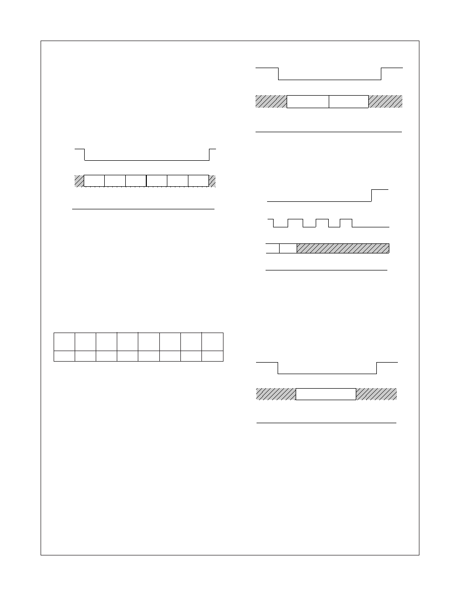
The FM25C041U is also capable of a 4 byte PAGE WRITE
operation. Page write is performed similar to byte write operation
described above. During a Page write operation, after the first byte
of data, additional bytes (up to 3 bytes) can be input, before
bringing the /CS pin high to start the programming. After receipt of
each byte of data, the EEPROM internally increments the two low
order address bits (A1-A0) by one. The high order address bits
(A8-A2) will remain constant. If the master should transmit more
than 4 bytes of data, the address counter (A1-A0) will “roll over”
and the previously loaded data will be reloaded. See
Figure 11.
FIGURE 11. Page Write
/CS
SI
SO
Write
Op-Code
Byte
Addr
Data
(1)
Data
(2)
Data
(3)
Data
(4)
/CS
SI
SO
WRSR
Op-Code
SR Data
xxxxBP1BP0xx
FIGURE 12. Write Status Register
BP0
SCK
SI
SO
/CS
SI
SO
INVALID CODE
At the completion of a write cycle the EEPROM is automatically
returned to the write disabled state. Note that if the EEPROM is not
write enabled (WEN=0) before issuing the WRITE instruction, the
EEPROM will ignore the WRITE instruction and return to the
standby state when /CS is brought high.
WRITE STATUS REGISTER (WRSR):
The Write Status Register (WRSR) instruction provides write
access to the status register. This instruction is used to set Block
Write protection to a portion of the array as defined under Table
4. During a WRSR instruction only Bit3 (BP1) and Bit2 (BP0) can
be written with valid information while other bits are ignored.
Following is the format of WRSR data:
Status Register Write Data
Bit
7
6
54
32
1
0
X
BP1
BP0
X
X = Don’t Care
Note that the first four bits are don’t care bits followed by BP1 and
BP0 and two more don’t care bits.
WRSR instruction is enabled only when /WP pin is held high and
the EEPROM is write enabled previously (via WREN instruction).
WRSR command requires the following sequence. The /CS pin is
pulled low to select the EEPROM and then the WRSR opcode is
transmitted on the SI pin followed by the data to be programmed.
See
Figure 12.
Programming will start after the /CS pin is forced back to a high
level. As in the WRITE instruction the LOW to HIGH transition of
the /CS pin must occur during the SCK low time immediately after
clocking in the last don’t care bit. See
Figure 13.
FIGURE 13. Start WRSR Condition
At the completion of this instruction the EEPROM is automatically
returned to write disabled state.
INVALID OPCODE
If an invalid code is received, then no data is shifted into the
EEPROM, and the SO data output pin remains high impedance
state until a new /CS falling edge reinitializes the serial communi-
cation. See
Figure 14.
FIGURE 14. Invalid Op-Code
相关PDF资料 |
PDF描述 |
|---|---|
| FM25C041ULZEN | SPI Serial EEPROM |
| FM25C041ULZMT8 | SPI Serial EEPROM |
| FMC1819C6-02 | 18700 MHz - 19700 MHz RF/MICROWAVE WIDE BAND LOW POWER AMPLIFIER |
| FMM5117X | 20-32GHz Downconverter MMIC |
| FMM5822X | 17500 MHz - 20000 MHz RF/MICROWAVE WIDE BAND MEDIUM POWER AMPLIFIER |
相关代理商/技术参数 |
参数描述 |
|---|---|
| FM25C041ULZEMT8 | 制造商:FAIRCHILD 制造商全称:Fairchild Semiconductor 功能描述:SERIAL EEPROM|512X8|CMOS|TSSOP|8PIN|PLASTIC |
| FM25C041ULZEN | 制造商:未知厂家 制造商全称:未知厂家 功能描述:SPI Serial EEPROM |
| FM25C041ULZM8 | 制造商:FAIRCHILD 制造商全称:Fairchild Semiconductor 功能描述:SERIAL EEPROM|512X8|CMOS|SOP|8PIN|PLASTIC |
| FM25C041ULZMT8 | 制造商:未知厂家 制造商全称:未知厂家 功能描述:SPI Serial EEPROM |
| FM25C041ULZN | 制造商:FAIRCHILD 制造商全称:Fairchild Semiconductor 功能描述:SERIAL EEPROM|512X8|CMOS|DIP|8PIN|PLASTIC |
发布紧急采购,3分钟左右您将得到回复。