- 您现在的位置:买卖IC网 > PDF目录296013 > FM25C041ULZEM8 SPI Serial EEPROM PDF资料下载
参数资料
| 型号: | FM25C041ULZEM8 |
| 英文描述: | SPI Serial EEPROM |
| 中文描述: | SPI串行EEPROM |
| 文件页数: | 9/11页 |
| 文件大小: | 101K |
| 代理商: | FM25C041ULZEM8 |
7
www.fairchildsemi.com
FM25C041U
FM25C041U
4K-Bit
SPI
Interface
Serial
CMOS
EEPROM
Functional Description (Continued)
SPI communication
As mentioned before, serial communication with the EEPROM is
enabled when the /CS pin is held low and the /HOLD pin is held
high. Input data (Instruction Opcodes, Array addresses and Data)
on the SI pin is latched in on the falling edges of SCK clock signal,
starting from the first falling edge after the /CS pin goes low. During
the time the SI data is input into the EEPROM, the SO pin remains
in high impedance state. If the intended instruction is of read
nature (Array read and Status register read), then data from the
EEPROM is driven out actively on the SO pin from every rising
edge of the SCK after the last input data (SI) is latched in. During
the time the SO data is output from the EEPROM, the data on the
SI pin is ignored.
Figure 2 illustrates the above. Refer Figure 1 for
timing information.
HOLD function
An active communication with the EEPROM can be temporarily
suspended by bringing the /HOLD pin low when a EEPROM is
selected (/CS pin should be low) and a serial sequence with the
EEPROM is currently underway. To suspend the communication,
/HOLD pin must be driven low while SCK is high, otherwise the
Hold function will not be invoked until the next SCK low to high
transition. The EEPROM must remain selected during this se-
quence. Transitions on the SCK and SI pins are ignored during the
time the part is suspended and the SO pin will be in high
impedance state. Releasing the /HOLD pin back to high state will
allow the operation to resume from the point it was suspended.
/HOLD pin must be driven high while the SCK pin is high,
otherwise serial communication will not resume until the next SCK
low to high transition. Asserting a low on the /HOLD pin at any time
will tri-state the SO pin.
Figure 3 illustrates Hold timing.
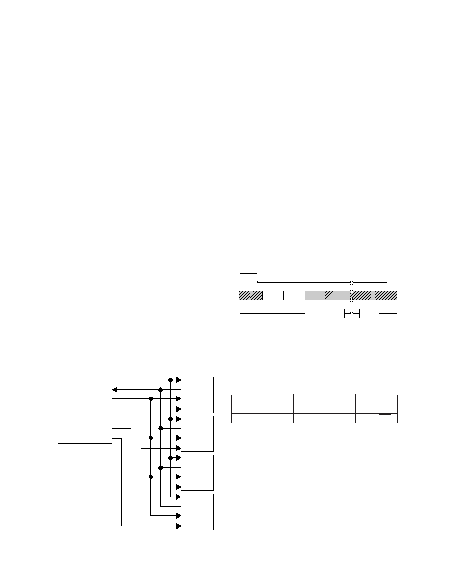
System Configuration
When multiple SPI peripherals (for e.g. EEPROMs) are present on
the bus, the SI, SO and the SCK signals can be tied together.
Figure 4 illustrates a typical system configuration with respect to
/CS, SCK, SI and SO pins.
FIGURE 4. System Configuration
SI
SO
SCK
/CS
DATA OUT (MOSI)
DATA IN (MISO)
SERIAL CLOCK (SPICK)
SS0
SS1
SS2
SS3
SI
SO
SCK
/CS
SI
SO
SCK
/CS
SI
SO
SCK
/CS
SELECTION
CHIP
SPI
MASTER MCU
FM25Cxxx
SPI Modes 1 and 2
FM25C041U supports both MODE 1 and MODE 2 of operations.
The difference between MODE 1 and MODE 2 is determined by
the state of the SCK clock signal when a SPI cycle starts (when /
CS is driven low) as well as when the SPI cycle ends (when /CS
is driven high). Under MODE 2 of operation, the SCK signal is held
low both at the start and at the end of a SPI cycle. Under Mode 1
of operation, the SCK signal is held high both at the start and at the
end of a SPI cycle. However in both of these two modes, the input
data (SI) is sampled (latched in) at the falling edge of the SCK
clock signal and the output data (SO) is driven after the rising edge
of the SCK clock signal. See
Figure 1 and Figure 2.
READ SEQUENCE (READ)
Reading the memory via the serial SPI link requires the following
sequence. The /CS pin is pulled low to select the EEPROM. The
READ opcode is transmitted on the SI pin followed by the byte
address (A7–A0) to be read. After this is done, data on the SI pin
becomes don’t care. The data (D7–D0) at the address specified is
then shifted out on the SO pin. If only one byte is to be read, the
/CS pin can be pulled back to the high level. It is possible to
continue the READ sequence as the byte address is automatically
incremented and data will continue to be shifted out as clock
pulses are continuously applied. When the end of memory array
is reached (last byte location), the address counter rolls over to the
start of memory array (first byte location) allowing the entire
memory to be read in one continuous READ cycle. See
Figure 5.
FIGURE 5. Read Sequence
/CS
SI
SO
Read
Opcode
Byte
Addr
Data
(1)
Data
(2)
Data
(n)
READ STATUS REGISTER (RDSR):
The Read Status Register (RDSR) instruction provides read
access to the status register. As mentioned before, of the 8bits of
data, only the LSB 4bits are valid and they indicate Block Protec-
tion information (BP1 and BP0), Write Enable status (WEN) and
Busy/Ready status (/RDY) of the EEPROM. MSB 4bits of are
invalid (Don’t cares) Following is the format of RDSR data:
TABLE 3. Status Register Format
Bit
7
6
54
32
1
0
X
BP1
BP0
WEN
RDY
Bit3 (BP1) and Bit2 (BP0) together indicate Block write protection
previously set on the EEPROM. Refer Table 2.
Bit1 (WEN) indicates the Write enable status of the EEPROM.
This bit is a read-only bit and is read by executing RDSR
instruction. If this bit is “1” then the EEPROM is write enabled. If
this bit is “0” then the EEPROM is write disabled.
Bit0 (/RDY) indicates the Busy/Ready status of the EEPROM.
This bit is a read-only bit and is read by executing RDSR
instruction. If this bit is “1” then the EEPROM is busy doing a
program cycle. If this bit is “0” then the EEPROM is ready.
Note that if a RDSR instruction is executed when an internal
programming cycle is in progress, only the /RDY bit is valid.
All other bits are don’t cares.
相关PDF资料 |
PDF描述 |
|---|---|
| FM25C041ULZEN | SPI Serial EEPROM |
| FM25C041ULZMT8 | SPI Serial EEPROM |
| FMC1819C6-02 | 18700 MHz - 19700 MHz RF/MICROWAVE WIDE BAND LOW POWER AMPLIFIER |
| FMM5117X | 20-32GHz Downconverter MMIC |
| FMM5822X | 17500 MHz - 20000 MHz RF/MICROWAVE WIDE BAND MEDIUM POWER AMPLIFIER |
相关代理商/技术参数 |
参数描述 |
|---|---|
| FM25C041ULZEMT8 | 制造商:FAIRCHILD 制造商全称:Fairchild Semiconductor 功能描述:SERIAL EEPROM|512X8|CMOS|TSSOP|8PIN|PLASTIC |
| FM25C041ULZEN | 制造商:未知厂家 制造商全称:未知厂家 功能描述:SPI Serial EEPROM |
| FM25C041ULZM8 | 制造商:FAIRCHILD 制造商全称:Fairchild Semiconductor 功能描述:SERIAL EEPROM|512X8|CMOS|SOP|8PIN|PLASTIC |
| FM25C041ULZMT8 | 制造商:未知厂家 制造商全称:未知厂家 功能描述:SPI Serial EEPROM |
| FM25C041ULZN | 制造商:FAIRCHILD 制造商全称:Fairchild Semiconductor 功能描述:SERIAL EEPROM|512X8|CMOS|DIP|8PIN|PLASTIC |
发布紧急采购,3分钟左右您将得到回复。