- 您现在的位置:买卖IC网 > PDF目录68995 > FMS2704LT1C (FAIRCHILD SEMICONDUCTOR CORP) SPECIALTY ANALOG CIRCUIT, PDSO24 PDF资料下载
参数资料
| 型号: | FMS2704LT1C |
| 厂商: | FAIRCHILD SEMICONDUCTOR CORP |
| 元件分类: | 模拟信号调理 |
| 英文描述: | SPECIALTY ANALOG CIRCUIT, PDSO24 |
| 封装: | TSSOP-24 |
| 文件页数: | 14/39页 |
| 文件大小: | 173K |
| 代理商: | FMS2704LT1C |
第1页第2页第3页第4页第5页第6页第7页第8页第9页第10页第11页第12页第13页当前第14页第15页第16页第17页第18页第19页第20页第21页第22页第23页第24页第25页第26页第27页第28页第29页第30页第31页第32页第33页第34页第35页第36页第37页第38页第39页
FMS2704/FMS2704L
PRODUCT SPECIFICATION
REV. 1.01 12/2/99
21
2.
If Conguration Register bit, TRIPLOCK = H
a) TL7-0 > PTL7-0.
b) TR17-0 > PTR7-0.
c) TR27-0 > PTR7-0.
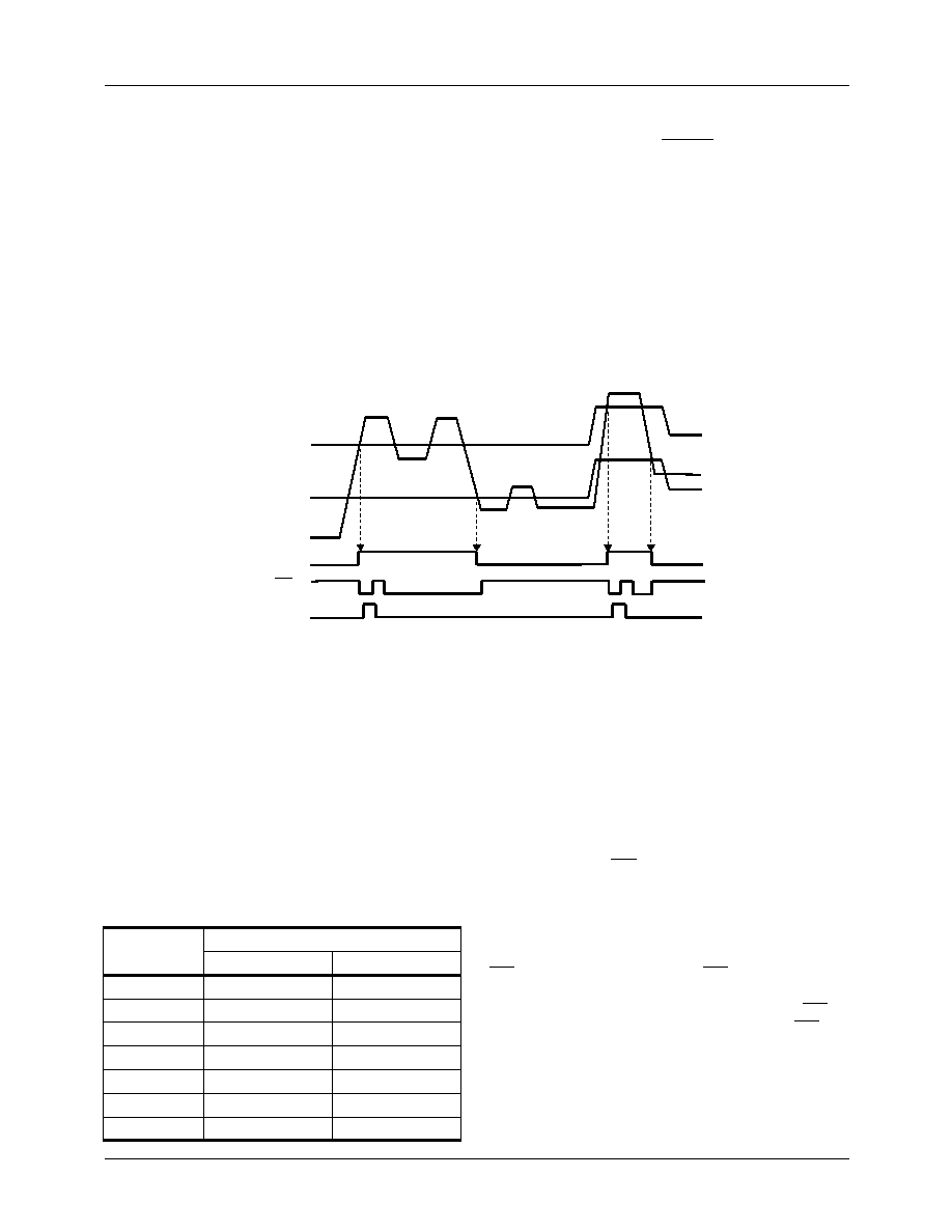
A typical THERM sequence is shown in Figure 5, which
depicts the prole of events when TR1 transitions through the
PTR trip point threshold. Similar proles apply to:
1.
TR1 with FTR limits
2.
TR2 with PTR and FTR trip points
3.
and to TL and TR2 with the appr
TRIPLOCK is Temperature Trip Point Lock bit in the Cong-
uration Register. After a Trip Point has been exceeded, to
restore the open drain output, THERM = Z, the temperature
must fall 5°C below the trip point.
Figure 5. Profile of THERM Driven Events
INT
TR1
PTR
PTR - 5
ITHERM
RD_INT
Voltage Monitoring
In the voltmeter mode, either diode input can become a pair
of single-ended voltage inputs. A low pass lter in each
input minimizes uctuations caused by noise riding on the
input signals. Voltmeter inputs are optimized for conversion
of a nominal 1000mV signal that is converted with a sensi-
tivity of 0.2 lsb/mV.
Voltmeter data format is 8-bit integer. Table 2 shows register
values corresponding to selected inputs. By setting the value
of VAVE, the number of samples to be averaged can be set to
be either 1, 2, 4, 8, 16, 32 or 64.
One set of high and low limit values, VHI7-0 and VLO7-0 are
shared between the six voltage values. Violation of a limit will
set the corresponding ag in the Voltage Error Register. Flag i
is set as a result of either of the following conditions:
1.
Vi < VLO
2.
Vi > VHI
Where i = 1:6.
If the ag is not masked by the Voltage Error Mask Register,
the Interrupt Output, INT = L. After the source of the error
has been identied, further interrupts can be prevented by
masking the source of the error.
Interrupt Processing
INT is a hardware interrupt output. INT operation is
controlled by the Conguration Register bits: INT_EN and
INT_CLR bits, which enable and clear the open drain INT
output. Subject to the setting of the Mask Registers, INT =L,
if any bit is active in the following registers:
1.
Tachometer Status.
2.
Voltage Status Register.
3.
Temperature Status Register.
Table 2. Voltage Conversion
Input (mV)
Voltage Value
Decimal
Hex
0
100
20
14
500
100
64
900
180
B4
1000
200
C8
1100
220
DC
1275
255
FF
相关PDF资料 |
PDF描述 |
|---|---|
| FMS2704T1C | SPECIALTY ANALOG CIRCUIT, PDSO24 |
| FMS6501MSA28X_NL | 12-CHANNEL, AUDIO/VIDEO SWITCH, PDSO28 |
| FN3000-810-830 | PLL FREQUENCY SYNTHESIZER, DMA37 |
| FNA41060 | AC MOTOR CONTROLLER, DMA26 |
| FNB41560 | AC MOTOR CONTROLLER, DMA26 |
相关代理商/技术参数 |
参数描述 |
|---|---|
| FMS2704MTC | 制造商:Fairchild Semiconductor Corporation 功能描述: |
| FMS2A | 制造商:ROHM Semiconductor 功能描述:100 mA, 40 V, 2 CHANNEL, PNP, Si, SMALL SIGNAL TRANSISTOR |
| FMS2T148 | 制造商:ROHM Semiconductor 功能描述: |
| FMS3 | 制造商:MITA 功能描述:12M COIL SA 38X16MM TRUNK |
| FMS300 | 制造商:Black Box Corporation 功能描述:CAT6 SHIELDED JACK 90 DEGREE |
发布紧急采购,3分钟左右您将得到回复。