- 您现在的位置:买卖IC网 > PDF目录68995 > FMS2704LT1C (FAIRCHILD SEMICONDUCTOR CORP) SPECIALTY ANALOG CIRCUIT, PDSO24 PDF资料下载
参数资料
| 型号: | FMS2704LT1C |
| 厂商: | FAIRCHILD SEMICONDUCTOR CORP |
| 元件分类: | 模拟信号调理 |
| 英文描述: | SPECIALTY ANALOG CIRCUIT, PDSO24 |
| 封装: | TSSOP-24 |
| 文件页数: | 17/39页 |
| 文件大小: | 173K |
| 代理商: | FMS2704LT1C |
第1页第2页第3页第4页第5页第6页第7页第8页第9页第10页第11页第12页第13页第14页第15页第16页当前第17页第18页第19页第20页第21页第22页第23页第24页第25页第26页第27页第28页第29页第30页第31页第32页第33页第34页第35页第36页第37页第38页第39页
PRODUCT SPECIFICATION
FMS2704/FMS2704L
24
REV. 1.01 12/2/99
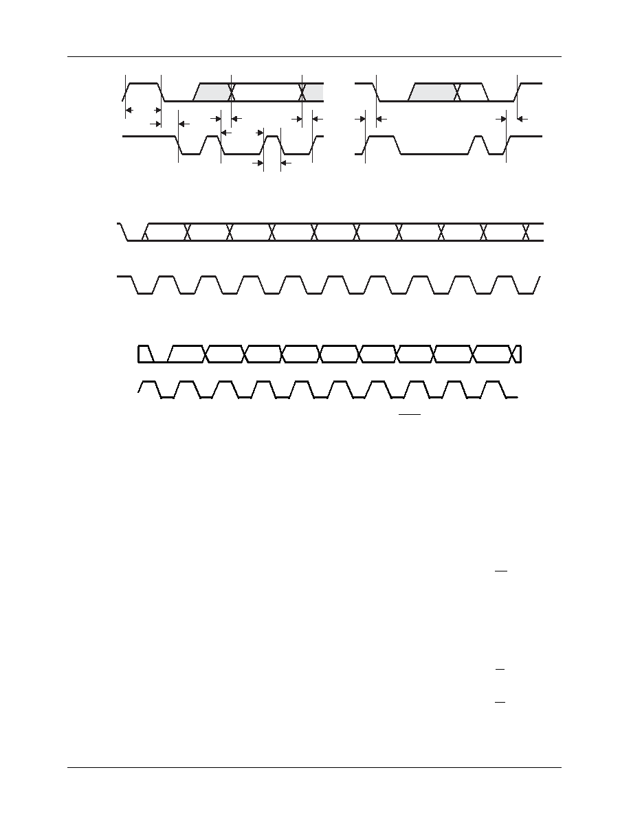
Figure 8. Serial Bus: Read/Write Timing
Figure 9. Serial Bus: Typical Byte Transfer
Figure 10. Serial Bus: Slave Address with Read/Write Bit
tBUFF
SDA
SCL
tSTAH
tDHO
tSU
tDAL
tDAH
tSTASU
tSTOSU
SDA
SCL
bit 7
bit 6
bit 5
bit 4
bit 3
bit 2
bit 1
bit 0
ACK
A6
A5
A4
A3
A2
A1
A0
R/W\
ACK
SDA
SCL
There are ve steps within an I2C/SMBus cycle:
1.
Start signal
2.
Slave address byte
3.
Pointer register address byte
4.
Data byte to read or write
5.
Stop signal
When the Serial Bus interface is inactive (SCL = H and SDA
= H) communications are initiated by sending a start signal.
The start signal (Figure 8, left waveform) is a HIGH-to-LOW
transition on SDA while SCL is HIGH. This signal alerts all
slaved devices that a data transfer sequence is imminent.
After a start signal, the rst eight bits of data that are transferred,
comprise a seven bit slave address followed a single R/W bit
(Read = H, Write = L). As shown in Figure 9, the R/W bit
indicates the direction of data transfer: read from; or write to
the slave device. If the transmitted slave address matches the
address of the FMS2704 which set by the state of the ADD
pin, the FMS2704 acknowledges by pulling SDA LOW on the
9th SCL pulse (see Figure 10). If the addresses do not match,
the FMS2704 does not acknowledge.
For each byte of data read or written, the MSB is the rst bit of
the sequence.
Data Transfer Via Serial Interface
If a slave device, such as the FMS2704 does not acknowledge
the master device during a write sequence, SDA remains
HIGH so the master can generate a stop signal. During a read
sequence, if the master device does not acknowledge (ACK
= L), the FMS2704 interprets this as “end of data.” SDA
remains HIGH so the master can generate a stop signal.
To write data to a specic FMS2704 control register, three
bytes are sent:
1.
Write the slave address byte with bit R/W = L.
2.
Write the pointer byte.
3.
Write to the control register indexed by the pointer.
Data is read from the control registers of the FMS2704 in a
similar manner, except that two data transfer operations are
required:
4.
Write the slave address byte with bit R/W = L.
5.
Write the pointer byte.
6.
Write the slave address byte with bit R/W = H
7.
Read the control register indexed by the pointer.
相关PDF资料 |
PDF描述 |
|---|---|
| FMS2704T1C | SPECIALTY ANALOG CIRCUIT, PDSO24 |
| FMS6501MSA28X_NL | 12-CHANNEL, AUDIO/VIDEO SWITCH, PDSO28 |
| FN3000-810-830 | PLL FREQUENCY SYNTHESIZER, DMA37 |
| FNA41060 | AC MOTOR CONTROLLER, DMA26 |
| FNB41560 | AC MOTOR CONTROLLER, DMA26 |
相关代理商/技术参数 |
参数描述 |
|---|---|
| FMS2704MTC | 制造商:Fairchild Semiconductor Corporation 功能描述: |
| FMS2A | 制造商:ROHM Semiconductor 功能描述:100 mA, 40 V, 2 CHANNEL, PNP, Si, SMALL SIGNAL TRANSISTOR |
| FMS2T148 | 制造商:ROHM Semiconductor 功能描述: |
| FMS3 | 制造商:MITA 功能描述:12M COIL SA 38X16MM TRUNK |
| FMS300 | 制造商:Black Box Corporation 功能描述:CAT6 SHIELDED JACK 90 DEGREE |
发布紧急采购,3分钟左右您将得到回复。