- 您现在的位置:买卖IC网 > Datasheet目录623 > FSB50825US (Fairchild Semiconductor)IC POWER MOD SPM 250V 4A SPM23BD Datasheet资料下载
参数资料
| 型号: | FSB50825US |
| 厂商: | Fairchild Semiconductor |
| 文件页数: | 4/9页 |
| 文件大小: | 0K |
| 描述: | IC POWER MOD SPM 250V 4A SPM23BD |
| 标准包装: | 1 |
| 系列: | SPM™ |
| 类型: | FET |
| 配置: | 3 相 |
| 电流: | 4A |
| 电压: | 250V |
| 电压 - 隔离: | 1500Vrms |
| 封装/外壳: | SPM23BD |
| 产品目录页面: | 1223 (CN2011-ZH PDF) |
| 其它名称: | FSB50825USDKR |
�� �
�
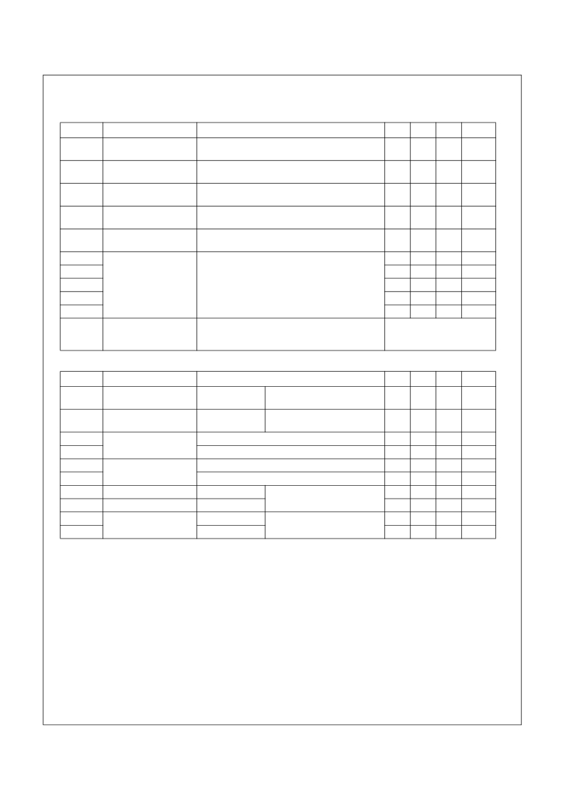
�Electrical� Characteristics� (T� J� =� 25°C,� V� CC� =� V� BS� =� 15� V� unless� otherwise� specified.)�
�Inverter� Part� (each� MOSFET� unless� otherwise� specified.)�
�Symbol�
�Parameter�
�Conditions�
�Min� Typ� Max�
�Unit�
�BV� DSS�
�?� BV� DSS� /�
�?� T� J�
�I� DSS�
�R� DS(on)�
�V� SD�
�t� ON�
�t� OFF�
�t� rr�
�E� ON�
�E� OFF�
�Drain� -� Source�
�Breakdown� Voltage�
�Breakdown� Voltage� Tem-�
�perature� Coefficient�
�Zero� Gate� Voltage�
�Drain� Current�
�Static� Drain� -� Source�
�Turn-On� Resistance�
�Drain� -� Source� Diode�
�Forward� Voltage�
�Switching� Times�
�V� IN� =� 0� V,� I� D� =� 1� mA� (2nd� Note� 1)�
�I� D� =� 250� ?� A,� Referenced� to� 25°C�
�V� IN� =� 0� V,� V� DS� =� 250� V�
�V� CC� =� V� BS� =� 15� V,� V� IN� =� 5� V,� I� D� =� 0.5� A�
�V� CC� =� V� BS� =� 15V,� V� IN� =� 0� V,� I� D� =� -0.5� A�
�V� PN� =� 150� V,� V� CC� =� V� BS� =� 15� V,� I� D� =� 0.5� A�
�V� IN� =� 0� V� ?� 5� V,� Inductive� Load� L� =� 3� mH�
�High-� and� Low-Side� MOSFET� Switching�
�(2nd� Note� 2)�
�250�
�-�
�-�
�-�
�-�
�-�
�-�
�-�
�-�
�-�
�-�
�0.31�
�-�
�-�
�-�
�1050�
�450�
�140�
�100�
�5�
�-�
�-�
�250�
�0.45�
�1.20�
�-�
�-�
�-�
�-�
�-�
�V�
�V�
�?� A�
�?�
�V�
�ns�
�ns�
�ns�
�?� J�
�?� J�
�RBSOA�
�Reverse� Bias� Safe� Oper-�
�ating� Area�
�V� PN� =� 200� V,� V� CC� =� V� BS� =� 15� V,� I� D� =� I� DP� ,� V� DS� =� BV� DSS� ,�
�T� J� =� 150°C�
�High-� and� Low-Side� MOSFET� Switching� (2nd� Note� 3)�
�Full� Square�
�Control� Part� (each� HVIC� unless� otherwise� specified.)�
�Symbol�
�Parameter�
�Conditions�
�Min� Typ� Max�
�Unit�
�I� QCC�
�I� QBS�
�Quiescent� V� CC� Current�
�Quiescent� V� BS� Current�
�V� CC� =� 15� V,�
�V� IN� =� 0� V�
�V� BS� =� 15� V,�
�V� IN� =� 0� V�
�Applied� Between� V� CC� and� COM�
�Applied� Between� V� B(U)� -� U,�
�V� B(V)� -� V,� V� B(W)� -� W�
�-�
�-�
�-�
�-�
�160�
�100�
�?� A�
�?� A�
�UV� CCD�
�UV� CCR�
�UV� BSD�
�UV� BSR�
�Low-Side� Under-Voltage�
�Protection� (Figure� 8)�
�High-Side� Under-Voltage�
�Protection� (Figure� 9)�
�V� CC� Under-Voltage� Protection� Detection� Level�
�V� CC� Under-Voltage� Protection� Reset� Level�
�V� BS� Under-Voltage� Protection� Detection� Level�
�V� BS� Under-Voltage� Protection� Reset� Level�
�7.4�
�8.0�
�7.4�
�8.0�
�8.0�
�8.9�
�8.0�
�8.9�
�9.4�
�9.8�
�9.4�
�9.8�
�V�
�V�
�V�
�V�
�V� IH�
�V� IL�
�I� IH�
�I� IL�
�ON� Threshold� Voltage�
�OFF� Threshold� Voltage�
�Input� Bias� Current�
�Logic� HIGH� Level�
�Logic� LOW� Level�
�V� IN� =� 5V�
�V� IN� =� 0V�
�Applied� between� IN� and� COM�
�Applied� between� IN� and� COM�
�3.0�
�-�
�-�
�-�
�-�
�-�
�10�
�-�
�-�
�0.8�
�20�
�2�
�V�
�V�
�?� A�
�?� A�
�2nd� Notes:�
�1.� BV� DSS� is� the� absolute� maximum� voltage� rating� between� drain� and� source� terminal� of� each� MOSFET� inside� Motion� SPM� ?� 5� product.� V� PN� should� be� sufficiently� less� than� this�
�value� considering� the� effect� of� the� stray� inductance� so� that� V� PN� should� not� exceed� BV� DSS� in� any� case.�
�2.� t� ON� and� t� OFF� include� the� propagation� delay� of� the� internal� drive� IC.� Listed� values� are� measured� at� the� laboratory� test� condition,� and� they� can� be� different� according� to� the� field�
�applications� due� to� the� effect� of� different� printed� circuit� boards� and� wirings.� Please� see� Figure� 4� for� the� switching� time� definition� with� the� switching� test� circuit� of� Figure� 5.�
�3.� The� peak� current� and� voltage� of� each� MOSFET� during� the� switching� operation� should� be� included� in� the� Safe� Operating� Area� (SOA).� Please� see� Figure� 5� for� the� RBSOA� test�
�circuit� that� is� same� as� the� switching� test� circuit.�
�?2010� Fairchild� Semiconductor� Corporation�
�FSB50825US� Rev.� C4�
�4�
�www.fairchildsemi.com�
�相关PDF资料 |
PDF描述 |
|---|---|
| FSB52006S | MODULE SPM SMART PWR SPM23-BA |
| FSBB15CH60C | IC POWER MOD SPM 600V SPM27CC |
| FSBB15CH60F | MODULE SPM 600V SPM27-CA |
| FSBB20CH60CL | SMART POWER MODULE 20A SPM27-CB |
| FSBB20CH60CT | MODULE ADV MOTION SPM SPM27-CC |
相关代理商/技术参数 |
参数描述 |
|---|---|
| FSB52006S | 功能描述:IGBT 模块 60V 1A 15kHz RoHS:否 制造商:Infineon Technologies 产品:IGBT Silicon Modules 配置:Dual 集电极—发射极最大电压 VCEO:600 V 集电极—射极饱和电压:1.95 V 在25 C的连续集电极电流:230 A 栅极—射极漏泄电流:400 nA 功率耗散:445 W 最大工作温度:+ 125 C 封装 / 箱体:34MM 封装: |
| FSB560 | 功能描述:两极晶体管 - BJT NPN Transistor Low Saturation RoHS:否 制造商:STMicroelectronics 配置: 晶体管极性:PNP 集电极—基极电压 VCBO: 集电极—发射极最大电压 VCEO:- 40 V 发射极 - 基极电压 VEBO:- 6 V 集电极—射极饱和电压: 最大直流电集电极电流: 增益带宽产品fT: 直流集电极/Base Gain hfe Min:100 A 最大工作温度: 安装风格:SMD/SMT 封装 / 箱体:PowerFLAT 2 x 2 |
| FSB560_01 | 制造商:FAIRCHILD 制造商全称:Fairchild Semiconductor 功能描述:NPN Low Saturation Transistor |
| FSB560_Q | 功能描述:两极晶体管 - BJT NPN Transistor Low Saturation RoHS:否 制造商:STMicroelectronics 配置: 晶体管极性:PNP 集电极—基极电压 VCBO: 集电极—发射极最大电压 VCEO:- 40 V 发射极 - 基极电压 VEBO:- 6 V 集电极—射极饱和电压: 最大直流电集电极电流: 增益带宽产品fT: 直流集电极/Base Gain hfe Min:100 A 最大工作温度: 安装风格:SMD/SMT 封装 / 箱体:PowerFLAT 2 x 2 |
| FSB560A | 功能描述:两极晶体管 - BJT NPN Transistor Low Saturation RoHS:否 制造商:STMicroelectronics 配置: 晶体管极性:PNP 集电极—基极电压 VCBO: 集电极—发射极最大电压 VCEO:- 40 V 发射极 - 基极电压 VEBO:- 6 V 集电极—射极饱和电压: 最大直流电集电极电流: 增益带宽产品fT: 直流集电极/Base Gain hfe Min:100 A 最大工作温度: 安装风格:SMD/SMT 封装 / 箱体:PowerFLAT 2 x 2 |
发布紧急采购,3分钟左右您将得到回复。