- 您现在的位置:买卖IC网 > PDF目录223860 > GS4576S09L-25 (GSI TECHNOLOGY) DDR DRAM, PBGA144 PDF资料下载
参数资料
| 型号: | GS4576S09L-25 |
| 厂商: | GSI TECHNOLOGY |
| 元件分类: | DRAM |
| 英文描述: | DDR DRAM, PBGA144 |
| 封装: | UBGA-144 |
| 文件页数: | 7/64页 |
| 文件大小: | 2691K |
| 代理商: | GS4576S09L-25 |
第1页第2页第3页第4页第5页第6页当前第7页第8页第9页第10页第11页第12页第13页第14页第15页第16页第17页第18页第19页第20页第21页第22页第23页第24页第25页第26页第27页第28页第29页第30页第31页第32页第33页第34页第35页第36页第37页第38页第39页第40页第41页第42页第43页第44页第45页第46页第47页第48页第49页第50页第51页第52页第53页第54页第55页第56页第57页第58页第59页第60页第61页第62页第63页第64页
Preliminary
GS4576S09/18L
Specifications cited are subject to change without notice. For latest documentation see http://www.gsitechnology.com.
Rev: 1.01 4/2011
15/64
2011, GSI Technology
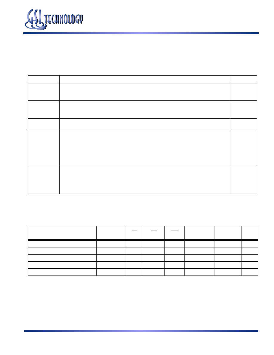
Commands
Valid control commands are listed below. Any input commands not shown are illegal or reserved. All inputs must meet
specified setup and hold times around the true crossing of CK.
Description of Commands
Command
Description
Notes
DSEL/NOP
The NOP command is used to perform a no operation to the LLDRAM II, which essentially deselects the
chip. Use the NOP command to prevent unwanted commands from being registered during idle or wait
states. Operations already in progress are not affected. Output values depend on command history.
1
MRS
The Mode Register is set via the address inputs A0–A17. See the Mode Register Definition diagrams for
further information. The MRS command can only be issued when all banks are idle and no bursts are in
progress.
—
READ
The Read command is used to initiate a burst read access to a bank. The value on the BA0–BA2 inputs
selects the bank, and the address provided on inputs A0–An selects the data location within the bank.
2
WRITE
The Write command is used to initiate a burst write access to a bank. The value on the BA0–BA2 inputs
selects the bank, and the address provided on inputs A0–An selects the data location within the bank.
Input data appearing on the Ds is written to the memory array subject to the DM input logic level
appearing coincident with the data. If the DM signal is registered Low, the corresponding data will be
written to memory. If the DM signal is registered High, the corresponding data inputs will be ignored (that
is, this part of the data word will not be written).
2
AREF
The AREF command is used during normal operation of the LLDRAM II to refresh the memory content
of a bank. The command is non-persistent, so it must be issued each time a refresh is required. The
value on the BA0–BA2 inputs selects the bank. The refresh address is generated by an internal refresh
controller, effectively making each address bit a “Don’t Care” during the AREF command.
See the Auto Refresh section for more details.
—
Notes:
1. When the chip is deselected, internal NOP commands are generated and no commands are accepted.
2. For the value of “n”, see Address Widths at Different Burst Lengths table.
Command Table
Operation
Command
CS
WE
REF
A0–An
BA0–BA2
No
tes
Device Deselect/No Operation
DSEL/NOP
H
X
1
MRS
L
CODE
X
1, 3
Read
READ
L
H
A
BA
1, 2
Write
WRITE
L
H
A
BA
1, 2
Auto Refresh
AREF
L
H
L
X
BA
1
Notes:
1. X= Don’t Care; H = Logic High; L = Logic Low; A = Valid Address; BA = Valid Bank Address.
2. For the value of “n”, see Address Widths at Different Burst Lengths table.
3. Only A0–A17 are used for the MRS command.
相关PDF资料 |
PDF描述 |
|---|---|
| GS54180RK | 1 ELEMENT, 18 uH, GENERAL PURPOSE INDUCTOR, SMD |
| GS54180RJ | 1 ELEMENT, 18 uH, GENERAL PURPOSE INDUCTOR, SMD |
| GS54180BL | 1 ELEMENT, 18 uH, GENERAL PURPOSE INDUCTOR, SMD |
| GS54151RL | 1 ELEMENT, 150 uH, GENERAL PURPOSE INDUCTOR, SMD |
| GS54151RK | 1 ELEMENT, 150 uH, GENERAL PURPOSE INDUCTOR, SMD |
相关代理商/技术参数 |
参数描述 |
|---|---|
| GS4576S18GL-24I | 制造商:GSI Technology 功能描述:32MB X 18 SEPARATE I/O - Trays |
| GS4576S18L-24I | 制造商:GSI Technology 功能描述:32MB X 18 SEPARATE I/O - Trays |
| GS4-6 | 制造商:JST Manufacturing 功能描述:CRIMP TERMINAL RING 4MM 制造商:JST Manufacturing 功能描述:CRIMP TERMINAL, RING, 4MM 制造商:JST Manufacturing 功能描述:CRIMP TERMINAL, RING, 4MM; Connector Type:Ring Tongue; Termination Method:Crimp; Stud/Tab Size:4mm; Wire Size AWG Min:12AWG; Wire Size AWG Max:10AWG; SVHC:No SVHC (19-Dec-2012); Cable Diameter Max:3.6mm; Stud Size:4mm; Wire Area Size;RoHS Compliant: Yes |
| GS4-6 BR TIN | 制造商:STIMPSON 功能描述: |
| GS4-6 BRASS | 制造商:STIMPSON 功能描述: |
发布紧急采购,3分钟左右您将得到回复。