- 您现在的位置:买卖IC网 > PDF目录383019 > GS8152Z18 (GSI TECHNOLOGY) 16Mb Pipelined and Flow Through Synchronous NBT SRAM(16M位流水线式和流通型同步NBT静态RAM) PDF资料下载
参数资料
| 型号: | GS8152Z18 |
| 厂商: | GSI TECHNOLOGY |
| 英文描述: | 16Mb Pipelined and Flow Through Synchronous NBT SRAM(16M位流水线式和流通型同步NBT静态RAM) |
| 中文描述: | 16Mb的流水线和流量,通过同步唑的SRAM(1,600位流水线式和流通型同步唑静态内存) |
| 文件页数: | 14/39页 |
| 文件大小: | 757K |
| 代理商: | GS8152Z18 |
第1页第2页第3页第4页第5页第6页第7页第8页第9页第10页第11页第12页第13页当前第14页第15页第16页第17页第18页第19页第20页第21页第22页第23页第24页第25页第26页第27页第28页第29页第30页第31页第32页第33页第34页第35页第36页第37页第38页第39页
Rev: 1.01 11/2000
Specifications cited are subject to change without notice. For latest documentation see http://www.gsitechnology.com.
14/39
2000, Giga Semiconductor, Inc.
Preliminary
GS8152Z18/36/72B-225/200/180/166/150/133
Burst Cycles
Although NBT RAMs are designed to sustain 100% bus bandwidth by eliminating turnaround cycle when there is transition from
read to write, multiple back-to-back reads or writes may also be performed. NBT SRAMs provide an on-chip burst address
generator that can be utilized, if desired, to further simplify burst read or write implementations. The ADV control pin, when
driven high, commands the SRAM to advance the internal address counter and use the counter generated address to read or write
the SRAM. The starting address for the first cycle in a burst cycle series is loaded into the SRAM by driving the ADV pin low, into
Load mode.
Burst Order
The burst address counter wraps around to its initial state after four addresses (the loaded address and three more) have been
accessed. The burst sequence is determined by the state of the Linear Burst Order pin (LBO). When this pin is Low, a linear burst
sequence is selected. When the RAM is installed with the LBO pin tied high, Interleaved burst sequence is selected. See the tables
below for details.
FLXDrive
The ZQ pin allows selection between NBT RAM nominal drive strength (ZQ low) for multi-drop bus applications and low drive
strength (ZQ floating or high) point-to-point applications. See the Output Driver Characteristics chart for details.
Mode Pin Functions
Note:
There areis a pull-up devices on the ZQ, SCD DP, and FT pins and a pull-down devices on the PE and ZZ pins, so those input pins
can be unconnected and the chip will operate in the default states as specified in the above tables.
Enable / Disable Parity I/O Pins
This SRAM allows the user to configure the device to operate in Parity I/O active (x18, x36, or x72) or in Parity I/O inactive (x16,
x32, or x64) mode. Holding the PE bump low or letting it float will activate the 9th I/O on each byte of the RAM. Grounding PE
deactivates the 9th I/O of each byte, although the bit in each byte of the memory array remains active to store and recall parity bits
generated and read into the ByteSafe parity circuits.
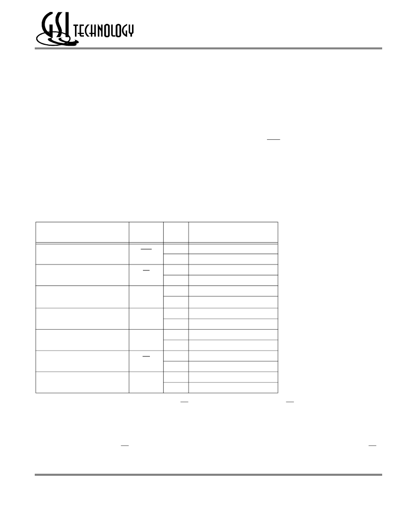
Mode Name
Pin
Name
State
Function
Burst Order Control
LBO
L
H
L
Linear Burst
Interleaved Burst
Flow Through
Pipeline
Active
Standby, I
DD
= I
SB
Dual Cycle Deselect
Single Cycle Deselect
Check for Odd Parity
Check for Even Parity
Activate 9th I/O’s (x18/36 Mode)
Deactivate 9th I/O’s (x16/32 Mode)
High Drive (Low Impedance)
Low Drive (High Impedance)
Output Register Control
FT
H or NC
L or NC
Power Down Control
ZZ
H
Single / Dual Cycle Deselect Control
SCD
L
H or NC
L
H or NC
L or NC
H
L
H or NC
ByteSafe Data Parity Control
DP
Parity Enable
PE
FLXDrive Output Impedance Control
ZQ
相关PDF资料 |
PDF描述 |
|---|---|
| GS8152Z36 | 16Mb Pipelined and Flow Through Synchronous NBT SRAM(16M位流水线式和流通型同步NBT静态RAM) |
| GS8152Z72 | 16Mb Pipelined and Flow Through Synchronous NBT SRAM(16M位流水线式和流通型同步NBT静态RAM) |
| GS816018 | 16Mb(1M x 18Bit)Sync Burst SRAM(16M位(1M x 18位)同步静态RAM(带2位脉冲地址计数器)) |
| GS816032 | 16Mb(512K x 36Bit)Sync Burst SRAM(16M位(512K x 36位)同步静态RAM(带2位脉冲地址计数器)) |
| GS816036 | 16Mb(256K x 72Bit)Sync Burst SRAM(16M位(256K x 72位)同步静态RAM(带2位脉冲地址计数器)) |
相关代理商/技术参数 |
参数描述 |
|---|---|
| GS815V018AB-250 | 制造商:GSI Technology 功能描述:GS815V018AB-250 - Trays |
| GS815V018AB-250I | 制造商:GSI Technology 功能描述:GS815V018AB-250I - Trays |
| GS815V018AB-300 | 制造商:GSI Technology 功能描述:GS815V018AB-300 - Trays |
| GS815V018AB-300I | 制造商:GSI Technology 功能描述:GS815V018AB-300I - Trays |
| GS815V018AB-333 | 制造商:GSI Technology 功能描述:GS815V018AB-333 - Trays |
发布紧急采购,3分钟左右您将得到回复。