- 您现在的位置:买卖IC网 > PDF目录223866 > GS8342D37BD-300I (GSI TECHNOLOGY) 1M X 36 QDR SRAM, 0.45 ns, PBGA165 PDF资料下载
参数资料
| 型号: | GS8342D37BD-300I |
| 厂商: | GSI TECHNOLOGY |
| 元件分类: | SRAM |
| 英文描述: | 1M X 36 QDR SRAM, 0.45 ns, PBGA165 |
| 封装: | 13 X 15 MM, 1 MM PITCH, FPBGA-165 |
| 文件页数: | 9/30页 |
| 文件大小: | 962K |
| 代理商: | GS8342D37BD-300I |
第1页第2页第3页第4页第5页第6页第7页第8页当前第9页第10页第11页第12页第13页第14页第15页第16页第17页第18页第19页第20页第21页第22页第23页第24页第25页第26页第27页第28页第29页第30页
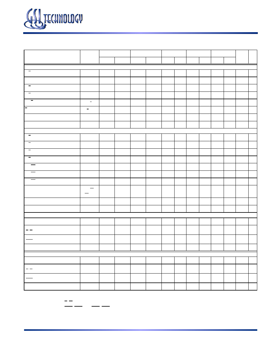
AC Electrical Characteristics
Parameter
Symbol
-450
-400
-350
-333
-300
Uni
ts
Not
es
Min
Max
Min
Max
Min
Max
Min
Max
Min
Max
Clock
K, K Clock Cycle Time
tKHKH
2.22
8.4
2.5
8.4
2.86
8.4
3.0
8.4
3.3
8.4
ns
tK Variable
tKVar
—
0.2
—
0.2
—
0.2
—
0.2
—
0.2
ns
4
K, K Clock High Pulse Width
tKHKL
0.4
—
0.4
—
0.4
—
0.4
—
0.4
—
cycle
K, K Clock Low Pulse Width
tKLKH
0.4
—
0.4
—
0.4
—
0.4
—
0.4
—
cycle
K to K High
tKHKH
0.94
—
1.06
—
1.13
—
1.28
—
1.32
—
ns
K to K High
tKHKH
0.94
—
1.06
—
1.13
—
1.28
—
1.32
—
ns
DLL Lock Time
tKLock
2048
—
2048
—
2048
—
2048
—
2048
—
cycle
5
K Static to DLL reset
tKReset
30
—
30
—
30
—
30
—
30
—
ns
Output Times
K, K Clock High to Data Output Valid
tKHQV
—
0.45
—
0.45
—
0.45
—
0.45
—
0.45
ns
K, K Clock High to Data Output Hold
tKHQX
–0.45
—
–0.45
—
–0.45
—
–0.45
—
–0.45
—
ns
K, K Clock High to Echo Clock Valid
tKHCQV
—
0.45
—
0.45
—
0.45
—
0.45
—
0.45
ns
K, K Clock High to Echo Clock Hold
tKHCQX
–0.45
—
–0.45
—
–0.45
—
–0.45
—
–0.45
—
ns
CQ, CQ High Output Valid
tCQHQV
—
0.15
—
0.2
—
0.23
—
0.25
—
0.27
ns
CQ, CQ High Output Hold
tCQHQX
–0.15
—
–0.2
—
–0.23
—
–0.25
—
–0.27
—
ns
CQ, CQ High to QVLD
tQVLD
–0.15
0.15
–0.2
0.2
–0.23
0.23
–0.25
0.25
–0.27
0.27
ns
CQ Phase Distortion
tCQHCQH
0.85
—
1.0
—
1.08
—
1.25
—
1.29
—
ns
K Clock High to Data Output High-Z
tKHQZ
—
0.45
—
0.45
—
0.45
—
0.45
—
0.45
ns
K Clock High to Data Output Low-Z
tKHQX1
–0.45
—
–0.45
—
–0.45
—
–0.45
—
–0.45
—
ns
Setup Times
Address Input Setup Time
tAVKH
0.275
—
0.4
—
0.4
—
0.4
—
0.4
—
ns
1
Control Input Setup Time
(R, W)
tIVKH
0.275
—
0.4
—
0.4
—
0.4
—
0.4
—
ns
2
Control Input Setup Time
(BWX)
tIVKH
0.22
—
0.28
—
0.28
—
0.28
—
0.28
—
ns
3
Data Input Setup Time
tDVKH
0.22
—
0.28
—
0.28
—
0.28
—
0.28
—
ns
Hold Times
Address Input Hold Time
tKHAX
0.275
—
0.4
—
0.4
—
0.4
—
0.4
—
ns
1
Control Input Hold Time
(R, W)
tKHIX
0.275
—
0.4
—
0.4
—
0.4
—
0.4
—
ns
2
Control Input Hold Time
(BWX)
tKHIX
0.22
—
0.28
—
0.28
—
0.28
—
0.28
—
ns
3
Data Input Hold Time
tKHDX
0.22
—
0.28
—
0.28
—
0.28
—
0.28
—
ns
Notes:
1. All Address inputs must meet the specified setup and hold times for all latching clock edges.
2. Control signals are R, W.
3. Control signals are BW0, BW1 and (BW2, BW3 for x36).
4. Clock phase jitter is the variance from clock rising edge to the next expected clock rising edge.
5. VDD slew rate must be less than 0.1 V DC per 50 ns for DLL lock retention. DLL lock time begins once VDD and input clock are stable.
Preliminary
GS8342D07/10/19/37BD-450/400/350/333/300
Specifications cited are subject to change without notice. For latest documentation see http://www.gsitechnology.com.
Rev: 1.00 4/2011
17/30
2011, GSI Technology
相关PDF资料 |
PDF描述 |
|---|---|
| GS8342QT07BD-357 | 4M X 8 QDR SRAM, 0.45 ns, PBGA165 |
| GS8342QT10BGD-300T | 4M X 9 QDR SRAM, 0.45 ns, PBGA165 |
| GS8342TT06BGD-500T | 4M X 8 DDR SRAM, 0.45 ns, PBGA165 |
| GS841Z36CGT-166IT | 128K X 36 ZBT SRAM, 7 ns, PQFP100 |
| GS842Z18CB-250T | 256K X 18 ZBT SRAM, 5.5 ns, PBGA119 |
相关代理商/技术参数 |
参数描述 |
|---|---|
| GS8342D38BD-350 | 制造商:GSI Technology 功能描述:165 FBGA - Bulk |
| GS8342D38BD-400 | 制造商:GSI Technology 功能描述:165 FBGA - Bulk |
| GS8342D38BD-450 | 制造商:GSI Technology 功能描述:165 FBGA - Bulk |
| GS8342D38BD-500 | 制造商:GSI Technology 功能描述:165 FBGA - Bulk |
| GS8342D38BD-550 | 制造商:GSI Technology 功能描述:165 FBGA - Bulk |
发布紧急采购,3分钟左右您将得到回复。