- 您现在的位置:买卖IC网 > Datasheet目录983 > HI5762EVAL2 (Intersil)EVALUATION MOD FOR HI5762 AMP Datasheet资料下载
参数资料
| 型号: | HI5762EVAL2 |
| 厂商: | Intersil |
| 文件页数: | 1/17页 |
| 文件大小: | 0K |
| 描述: | EVALUATION MOD FOR HI5762 AMP |
| 标准包装: | 1 |
| ADC 的数量: | 2 |
| 位数: | 10 |
| 采样率(每秒): | 60M |
| 数据接口: | 并联 |
| 输入范围: | 1 Vpp |
| 在以下条件下的电源(标准): | 650mW @ 60MSPS |
| 工作温度: | -40°C ~ 85°C |
| 已用 IC / 零件: | HI5762 |
| 已供物品: | 板 |
�� �
�
�HI5762EVAL2� Evaluation� Board� User’s� Manual�
�TM�
�Description�
�Application� Note�
�January� 1999�
�AN9811�
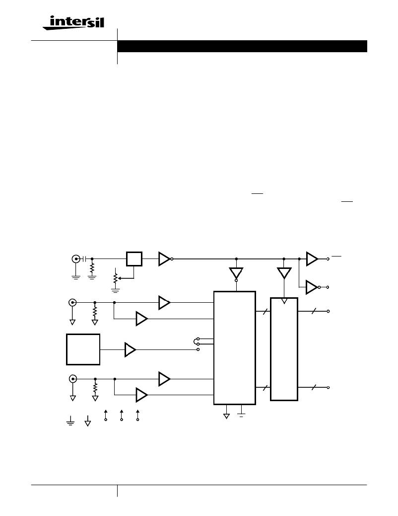
�The� HI5762EVAL2� evaluation� board� is� made� available� to�
�allow� the� circuit� designer� the� ability� to� evaluate� the�
�performance� of� the� Intersil� HI5762� monolithic� Dual� 10-bit� 60�
�MSPS� analog-to-digital� converter� (ADC)� with� internal�
�voltage� reference.� As� shown� in� the� Evaluation� Board�
�Functional� Block� Diagram,� this� evaluation� board� includes�
�sample� clock� generation� circuitry,� a� single-ended� to�
�differential� analog� input� ampli?er� con?guration� for� both� the� I�
�and� Q� channel� inputs,� an� external� variable� voltage� reference�
�and� digital� data� output� latches/buffers.� The� buffered� digital�
�data� outputs� are� conveniently� provided� for� easy� interfacing�
�to� a� ribbon� connector� or� logic� probes.�
�The� sample� clock� generator� circuit� accepts� the� external�
�sampling� signal� through� an� SMA� type� RF� connector,� J3.� This�
�input� is� AC-coupled� and� terminated� in� 50� ?� allowing� for�
�connection� to� most� laboratory� signal� generators.� In� addition,�
�the� duty� cycle� of� the� clock� driving� the� A/D� converter� is� made�
�Evaluation� Board� Functional� Block� Diagram�
�adjustable� by� way� of� a� potentiometer� so� that� the� effects� of�
�sample� clock� duty� cycle� on� the� HI5762� may� be� observed.�
�The� I� and� Q� channel� analog� input� signals� are� also� connected�
�through� SMA� type� RF� connectors,� J1� and� J2,� and� applied� to�
�single-ended� to� differential� analog� input� ampli?ers.� These�
�inputs� are� AC-coupled� and� terminated� in� 50� ?� allowing� for�
�connection� to� most� laboratory� signal� generators.� Also,�
�provisions� for� differential� RC� lowpass� ?lters� are� incorporated�
�on� the� output� of� the� differential� ampli?ers� to� limit� the�
�broadband� noise� going� into� the� HI5762� converter.�
�The� I� and� Q� channel� digital� data� output� latches/buffers�
�consist� of� a� pair� of� 74FCT2821� D-type� ?ip-?ops.� The� digital�
�data� output� interface� provides� both� phases� of� the� sampling�
�clock,� CLK� and� CLK,� so� that� the� digital� data� transitions� are�
�essentially� time� aligned� with� the� rising� edge� of� the� CLK�
�sampling� clock� or� time� aligned� with� the� falling� edge� of� the�
�CLK� sampling� clock.�
�SAMPLE�
�CLOCK�
�INPUT�
�J3�
�50� ?�
�+5V� D�
�BIAS�
�TEE�
�CLK�
�CLOCK�
�OUT�
�CLK�
�Q-CHANNEL�
�ANALOG�
�INPUT�
�(Q_IN)�
�J2�
�50� ?�
�G� =� -1�
�G� =� +1�
�QI� IN� +�
�QI� IN� -�
�CLK�
�QD� 0� -QD� 9�
�10�
�D�
�Q�
�10�
�Q-CHANNEL�
�DIGITAL�
�DATA�
�OUTPUT�
�(QD0� -� QD9)�
�ICL8069�
�V� ROUT�
�1.2V�
�BANDGAP�
�VOLTAGE�
�REFERENCE�
�VAR� GAIN�
�+2.5V�
�V� RIN�
�HI5762�
�I-CHANNEL�
�ANALOG�
�INPUT�
�(I_IN)�
�J1�
�50� ?�
�G� =� -1�
�G� =� +1�
�I� IN� +�
�I� IN� -�
�ID� 0� -ID� 9�
�10�
�D�
�Q�
�10�
�I-CHANNEL�
�DIGITAL�
�DATA�
�OUTPUT�
�(ID0� -� ID9)�
�DGND�
�AGND�
�+5V� D�
�+5V� A�
�-5V� A�
�3-1�
�1-888-INTERSIL� or� 321-724-7143�
�|�
�Intersil� and� Design� is� a� trademark� of� Intersil� Corporation.�
�|�
�Copyright�
�?� Intersil� Corporation� 2000�
�相关PDF资料 |
PDF描述 |
|---|---|
| HI5767EVAL1 | EVALUATION PLATFORM HI5767 |
| HI5767EVAL2 | EVALUATION PLATFORM HI5767 |
| HI5805EVAL1 | EVALUATION PLATFORM HI5805 |
| HI5828EVAL2 | EVALUATION PLATFORM HI5828 |
| HI5960SOICEVAL1 | EVALUATION PLATFORM SOIC HI5960 |
相关代理商/技术参数 |
参数描述 |
|---|---|
| HI5766 | 制造商:INTERSIL 制造商全称:Intersil Corporation 功能描述:10-Bit, 60 MSPS A/D Converter |
| HI5766_05 | 制造商:INTERSIL 制造商全称:Intersil Corporation 功能描述:10-Bit, 60MSPS A/D Converter |
| HI5766EVAL1 | 制造商:Rochester Electronics LLC 功能描述:- Bulk 制造商:Harris Corporation 功能描述: |
| HI5766KCA | 功能描述:IC ADC 10-BIT 60MSPS 28-SSOP RoHS:否 类别:集成电路 (IC) >> 数据采集 - 模数转换器 系列:- 产品培训模块:Lead (SnPb) Finish for COTS Obsolescence Mitigation Program 标准包装:2,500 系列:- 位数:12 采样率(每秒):3M 数据接口:- 转换器数目:- 功率耗散(最大):- 电压电源:- 工作温度:- 安装类型:表面贴装 封装/外壳:SOT-23-6 供应商设备封装:SOT-23-6 包装:带卷 (TR) 输入数目和类型:- |
| HI5766KCAZ | 功能描述:模数转换器 - ADC A/D 10-BIT 60MSPS 28 SSOP COM TEMP RoHS:否 制造商:Texas Instruments 通道数量:2 结构:Sigma-Delta 转换速率:125 SPs to 8 KSPs 分辨率:24 bit 输入类型:Differential 信噪比:107 dB 接口类型:SPI 工作电源电压:1.7 V to 3.6 V, 2.7 V to 5.25 V 最大工作温度:+ 85 C 安装风格:SMD/SMT 封装 / 箱体:VQFN-32 |
发布紧急采购,3分钟左右您将得到回复。