- 您现在的位置:买卖IC网 > Datasheet目录983 > HI5762EVAL2 (Intersil)EVALUATION MOD FOR HI5762 AMP Datasheet资料下载
参数资料
| 型号: | HI5762EVAL2 |
| 厂商: | Intersil |
| 文件页数: | 14/17页 |
| 文件大小: | 0K |
| 描述: | EVALUATION MOD FOR HI5762 AMP |
| 标准包装: | 1 |
| ADC 的数量: | 2 |
| 位数: | 10 |
| 采样率(每秒): | 60M |
| 数据接口: | 并联 |
| 输入范围: | 1 Vpp |
| 在以下条件下的电源(标准): | 650mW @ 60MSPS |
| 工作温度: | -40°C ~ 85°C |
| 已用 IC / 零件: | HI5762 |
| 已供物品: | 板 |
�� �
�
�Application� Note� 9811�
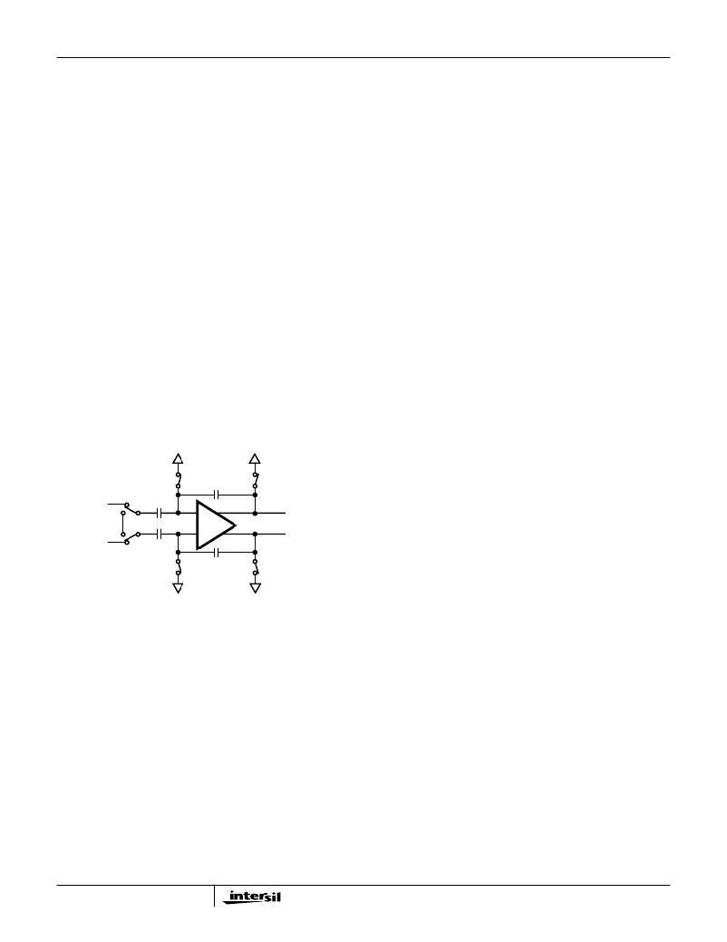
�Appendix� D� HI5762� A/D� Theory� of� Operation�
�The� HI5762� is� a� dual� 10-bit� fully� differential� sampling� pipeline�
�A/D� converter� with� digital� error� correction� logic.� Figure� 22�
�depicts� the� circuit� for� the� front� end� differential-in-differential-�
�out� sample-and-hold� (S/H)� ampli?ers.� The� switches� are�
�controlled� by� an� internal� sampling� clock� which� is� a� non-�
�overlapping� two� phase� signal,� Φ� 1� and� Φ� 2� ,� derived� from� the�
�master� sampling� clock.� During� the� sampling� phase,� Φ� 1� ,� the�
�input� signal� is� applied� to� the� sampling� capacitors,� C� S� .� At� the�
�same� time� the� holding� capacitors,� C� H� ,� are� discharged� to�
�analog� ground.� At� the� falling� edge� of� Φ� 1� the� input� signal� is�
�sampled� on� the� bottom� plates� of� the� sampling� capacitors.� In�
�the� next� clock� phase,� Φ� 2� ,� the� two� bottom� plates� of� the�
�sampling� capacitors� are� connected� together� and� the� holding�
�capacitors� are� switched� to� the� op� amp� output� nodes.� The�
�charge� then� redistributes� between� C� S� and� C� H� completing�
�one� sample-and-hold� cycle.� The� front� end� sample-and-hold�
�output� is� a� fully-differential,� sampled-data� representation� of�
�the� analog� input.� The� circuit� not� only� performs� the� sample-�
�and-hold� function� but� will� also� convert� a� single-ended� input�
�to� a� fully-differential� output� for� the� converter� core.� During� the�
�sampling� phase,� the� I/QI� N� pins� see� only� the� on-resistance� of�
�a� switch� and� C� S� .� The� relatively� small� values� of� these�
�components� result� in� a� typical� full� power� input� bandwidth� of�
�controlled� by� the� internal� sampling� clock.� The� function� of� the�
�digital� delay� line� is� to� time� align� the� digital� outputs� of� the� eight�
�identical� two-bit� subconverter� stages� with� the� corresponding�
�output� of� the� ninth� stage� flash� converter� before� applying� the�
�eighteen� bit� result� to� the� digital� error� correction� logic.� The�
�digital� error� correction� logic� uses� the� supplementary� bits� to�
�correct� any� error� that� may� exist� before� generating� the� final� ten�
�bit� digital� data� output� of� the� converter.�
�Because� of� the� pipeline� nature� of� this� converter,� the� digital�
�data� representing� an� analog� input� sample� is� output� to� the�
�digital� data� bus� following� the� 6th� cycle� of� the� clock� after� the�
�analog� sample� is� taken� (see� the� timing� diagram� in� Figure�
�24).� This� time� delay� is� specified� as� the� data� latency.� After�
�the� data� latency� time,� the� digital� data� representing� each�
�succeeding� analog� sample� is� output� during� the� following�
�clock� cycle.� The� digital� output� data� is� provided� in� offset�
�binary� format.�
�Internal� Reference� Voltage� Output,� V� REFOUT�
�The� HI5762� is� equipped� with� an� internal� reference� voltage�
�generator,� therefore,� no� external� reference� voltage� is�
�required.� V� ROUT� must� be� connected� to� V� RIN� when� using� the�
�internal� reference� voltage.�
�250MHz� for� the� converter.�
�An� internal� band-gap� reference� voltage� followed� by� an�
�amplifier/buffer� generates� the� precision� +2.5V� reference�
�voltage� used� by� the� converter.� A� band-gap� reference� circuit�
�Φ� 1�
�C� H�
�Φ� 1�
�is� used� to� generate� a� precision� +1.25V� internal� reference�
�I/Q� IN+�
�I/Q� IN-�
�Φ� 1�
�Φ� 2�
�Φ� 1�
�C� S�
�C� S�
�Φ� 1�
�-� +�
�+� -�
�C� H�
�Φ� 1�
�V� OUT+�
�V� OUT-�
�voltage.� This� voltage� is� then� amplified� by� a� wideband�
�uncompensated� operational� amplifier� connected� in� a�
�gain-of-two� configuration.� An� external,� user-supplied,�
�0.1� μ� F� capacitor� connected� from� the� V� ROUT� output� pin� to�
�analog� ground� is� used� to� set� the� dominant� pole� and� to�
�maintain� the� stability� of� the� operational� amplifier.�
�Reference� Voltage� Input,� V� REFIN�
�The� HI5762� is� designed� to� accept� a� +2.5V� reference� voltage�
�FIGURE� 22.� ANALOG� INPUT� SAMPLE-AND-HOLD�
�As� illustrated� in� the� functional� block� diagram� and� the� timing�
�diagram� in� Figures� 23� and� 24,� eight� identical� pipeline�
�subconverter� stages,� each� containing� a� two-bit� ?ash�
�converter� and� a� two-bit� multiplying� digital-to-analog�
�converter,� follow� the� S/H� circuit� with� the� ninth� stage� being� a�
�two� bit� ?ash� converter.� Each� converter� stage� in� the� pipeline�
�will� be� sampling� in� one� phase� and� amplifying� in� the� other�
�clock� phase.� Each� individual� subconverter� clock� signal� is�
�offset� by� 180� degrees� from� the� previous� stage� clock� signal�
�resulting� in� alternate� stages� in� the� pipeline� performing� the�
�same� operation.�
�The� output� of� each� of� the� eight� identical� two-bit� subconverter�
�stages� is� a� two-bit� digital� word� containing� a� supplementary� bit�
�to� be� used� by� the� digital� error� correction� logic.� The� output� of�
�each� subconverter� stage� is� input� to� a� digital� delay� line� which� is�
�3-14�
�source� at� the� V� RIN� input� pin.� Typical� operation� of� the�
�converter� requires� V� RIN� to� be� set� at� +2.5V.� The� HI5762� is�
�tested� with� V� RIN� connected� to� V� ROUT� yielding� a� fully�
�differential� analog� input� voltage� range� of� ±� 0.5V.�
�The� user� does� have� the� option� of� supplying� an� external�
�+2.5V� reference� voltage.� As� a� result� of� the� high� input�
�impedance� presented� at� the� V� RIN� input� pin,� 1.25k� ?� typically,�
�the� external� reference� voltage� being� used� is� only� required� to�
�source� 2mA� of� reference� input� current.� In� the� situation� where�
�an� external� reference� voltage� will� be� used� an� external� 0.1� μ� F�
�capacitor� must� be� connected� from� the� V� ROUT� output� pin� to�
�analog� ground� in� order� to� maintain� the� stability� of� the� internal�
�operational� ampli?er.�
�In� order� to� minimize� overall� converter� noise� it� is�
�recommended� that� adequate� high� frequency� decoupling� be�
�provided� at� the� reference� voltage� input� pin,� V� RIN� .�
�相关PDF资料 |
PDF描述 |
|---|---|
| HI5767EVAL1 | EVALUATION PLATFORM HI5767 |
| HI5767EVAL2 | EVALUATION PLATFORM HI5767 |
| HI5805EVAL1 | EVALUATION PLATFORM HI5805 |
| HI5828EVAL2 | EVALUATION PLATFORM HI5828 |
| HI5960SOICEVAL1 | EVALUATION PLATFORM SOIC HI5960 |
相关代理商/技术参数 |
参数描述 |
|---|---|
| HI5766 | 制造商:INTERSIL 制造商全称:Intersil Corporation 功能描述:10-Bit, 60 MSPS A/D Converter |
| HI5766_05 | 制造商:INTERSIL 制造商全称:Intersil Corporation 功能描述:10-Bit, 60MSPS A/D Converter |
| HI5766EVAL1 | 制造商:Rochester Electronics LLC 功能描述:- Bulk 制造商:Harris Corporation 功能描述: |
| HI5766KCA | 功能描述:IC ADC 10-BIT 60MSPS 28-SSOP RoHS:否 类别:集成电路 (IC) >> 数据采集 - 模数转换器 系列:- 产品培训模块:Lead (SnPb) Finish for COTS Obsolescence Mitigation Program 标准包装:2,500 系列:- 位数:12 采样率(每秒):3M 数据接口:- 转换器数目:- 功率耗散(最大):- 电压电源:- 工作温度:- 安装类型:表面贴装 封装/外壳:SOT-23-6 供应商设备封装:SOT-23-6 包装:带卷 (TR) 输入数目和类型:- |
| HI5766KCAZ | 功能描述:模数转换器 - ADC A/D 10-BIT 60MSPS 28 SSOP COM TEMP RoHS:否 制造商:Texas Instruments 通道数量:2 结构:Sigma-Delta 转换速率:125 SPs to 8 KSPs 分辨率:24 bit 输入类型:Differential 信噪比:107 dB 接口类型:SPI 工作电源电压:1.7 V to 3.6 V, 2.7 V to 5.25 V 最大工作温度:+ 85 C 安装风格:SMD/SMT 封装 / 箱体:VQFN-32 |
发布紧急采购,3分钟左右您将得到回复。