- 您现在的位置:买卖IC网 > PDF目录385381 > HI5804 (Intersil Corporation) 12-Bit, 5 MSPS A/D Converter PDF资料下载
参数资料
| 型号: | HI5804 |
| 厂商: | Intersil Corporation |
| 英文描述: | 12-Bit, 5 MSPS A/D Converter |
| 中文描述: | 12位,5 MSPS的A / D转换 |
| 文件页数: | 7/11页 |
| 文件大小: | 64K |
| 代理商: | HI5804 |
7
HI5804
Detailed Description
Theory of Operation
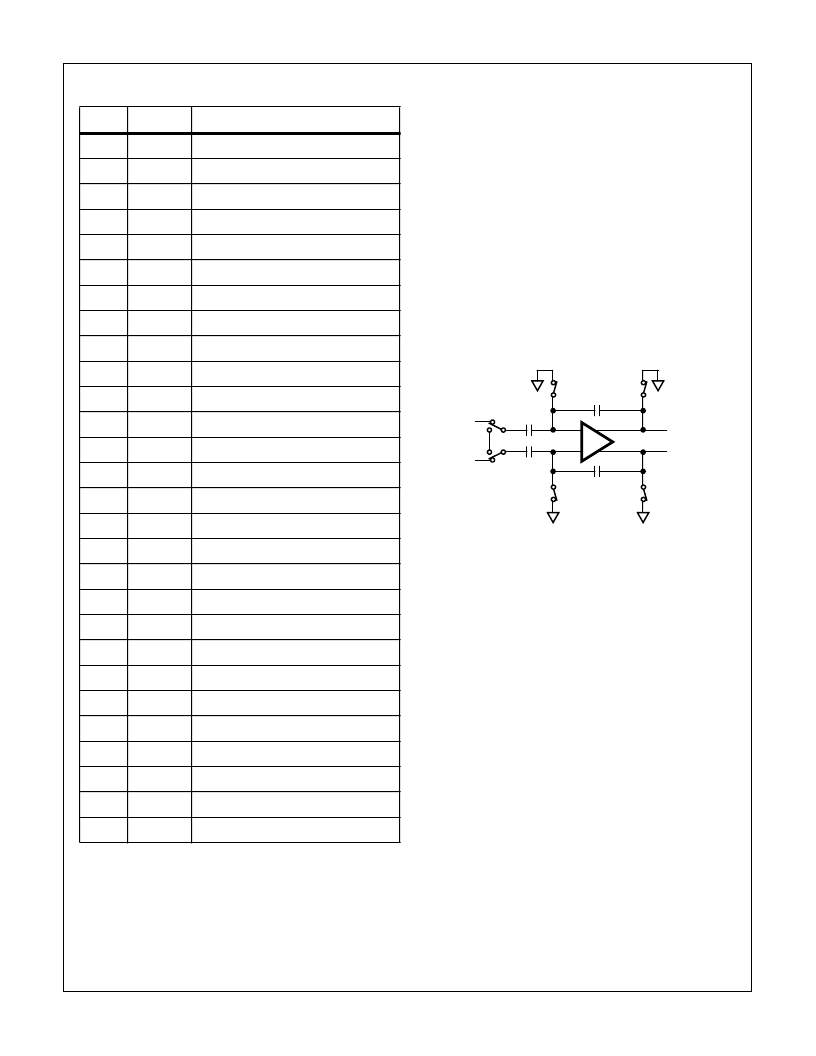
The HI5804 is a 12-bit, fully-differential, sampling pipeline
A/D converter with digital error correction. Figure 9 depicts
the circuit for the front end differential-in-differential-out sam-
ple-and-hold (S/H). The switches are controlled by an internal
clock which is a non-overlapping two phase signal
, φ
1
and
φ
2
,
derived from the master clock. During the sampling phase,
φ
1
, the input signal is applied to the sampling capacitors, C
S
.
At the same time the holding capacitors, C
H
, are discharged
to analog ground. At the falling edge of
φ
1
the input signal is
sampled on the bottom plates of the sampling capacitors. In
the next clock phase,
φ
2
, the two bottom plates of the sam-
pling capacitors are connected together and the holding
capacitors are switched to the op-amp output nodes. The
charge then redistributes between C
S
and C
H
completing one
sample-and-hold cycle. The output is a fully-differential, sam-
pled-data representation of the analog input. The circuit not
only performs the sample-and-hold function but will also con-
vert a single-ended input to a fully-differential output for the
converter core. During the sampling phase, the V
IN
pins see
only the on-resistance of a switch and C
S
. The relatively
small values of these components result in a typical full
power input bandwidth of 100MHz for the converter.
As illustrated in the functional block diagram and the timing
diagram in Figure 1, three identical pipeline subconverter
stages, each containing a four-bit flash converter, a four-bit
digital-to-analog converter and an amplifier with a voltage
gain of 8, follow the S/H circuit with the fourth stage being
only a four bit flash converter. Each converter stage in the
pipeline will be sampling in one phase and amplifying in the
other clock phase. Each individual sub-converter clock sig-
nal is offset by 180 degrees from the previous stage clock
signal with the result that alternate stages in the pipeline will
perform the same operation.
The 4-bit digital output of each stage is fed to a digital delay
line controlled by the internal clock. The purpose of the delay
line is to align the digital output data to the corresponding
sampled analog input signal. This delayed data is fed to the
digital error correction circuit which corrects the error in the
output data with the information contained in the redundant
bits to form the final twelve bit output for the converter.
Because of the pipeline nature of this converter, the data on
the bus is output at the 3rd cycle of the clock after the analog
sample is taken. This delay is specified as the data latency.
After the data latency time, the data representing each suc-
ceeding sample is output at the following clock pulse. The
output data is synchronized to the external clock by a latch.
The digital outputs are in offset binary format (See Table 1).
Pin Descriptions
PIN #
NAME
DESCRIPTION
1
CLK
Sample Clock Input.
2
DV
CC1
Digital Supply (+5.0V).
3
DGND1
Digital Ground.
4
DV
CC1
Digital Supply (+5.0V).
5
DGND1
Digital Ground.
6
AV
CC
Analog Supply (+5.0V).
7
AGND
Analog Ground.
8
V
IN
+
Positive Analog Input.
9
V
IN
-
Negative Analog Input.
10
V
DC
DC Bias Voltage Output.
11
V
ROUT
Reference Voltage Output.
12
V
RIN
Reference Voltage Input.
13
AGND
Analog Ground.
14
AV
CC
Analog Supply (+5.0V).
15
D11
Data Bit 11 Output (MSB).
16
D10
Data Bit 10 Output.
17
D9
Data Bit 9 Output.
18
D8
Data Bit 8 Output.
19
D7
Data Bit 7 Output.
20
D6
Data Bit 6 Output.
21
DGND2
Digital Output Ground.
22
DV
CC2
Digital Output Supply (+3.0V to +5.0V).
23
D5
Data Bit 5 Output.
24
D4
Data Bit 4 Output.
25
D3
Data Bit 3 Output.
26
D2
Data Bit 2 Output.
27
D1
Data Bit 1 Output.
28
D0
Data Bit 0 Output (LSB).
C
H
C
S
C
S
V
IN
+
V
OUT
+
V
OUT
-
V
IN
-
φ
1
φ
1
φ
2
φ
1
φ
1
-
+
+
-
C
H
φ
1
φ
1
FIGURE 9. ANALOG INPUT SAMPLE-AND-HOLD
相关PDF资料 |
PDF描述 |
|---|---|
| HI5804EVAL | 12-Bit, 5 MSPS A/D Converter |
| HI5804KCB | 12-Bit, 5 MSPS A/D Converter |
| HI5812JIB | CMOS 20 Microsecond, 12-Bit, Sampling A/D Converter with Internal Track and Hold |
| HI5812JIJ | CMOS 20 Microsecond, 12-Bit, Sampling A/D Converter with Internal Track and Hold |
| HI5812JIP | CMOS 20 Microsecond, 12-Bit, Sampling A/D Converter with Internal Track and Hold |
相关代理商/技术参数 |
参数描述 |
|---|---|
| HI5804EVAL | 制造商:Rochester Electronics LLC 功能描述:- Bulk 制造商:Harris Corporation 功能描述: |
| hi5804kcb | 制造商:Rochester Electronics LLC 功能描述:- Bulk 制造商:Harris Corporation 功能描述: |
| HI5805 | 制造商:INTERSIL 制造商全称:Intersil Corporation 功能描述:12-Bit, 5MSPS A/D Converter |
| HI5805_05 | 制造商:INTERSIL 制造商全称:Intersil Corporation 功能描述:12-Bit, 5MSPS A/D Converter |
| HI5805BIB | 功能描述:IC ADC 12-BIT 5MSPS 28-SOIC RoHS:否 类别:集成电路 (IC) >> 数据采集 - 模数转换器 系列:- 产品培训模块:Lead (SnPb) Finish for COTS Obsolescence Mitigation Program 标准包装:2,500 系列:- 位数:12 采样率(每秒):3M 数据接口:- 转换器数目:- 功率耗散(最大):- 电压电源:- 工作温度:- 安装类型:表面贴装 封装/外壳:SOT-23-6 供应商设备封装:SOT-23-6 包装:带卷 (TR) 输入数目和类型:- |
发布紧急采购,3分钟左右您将得到回复。