- 您现在的位置:买卖IC网 > PDF目录385381 > HI5804 (Intersil Corporation) 12-Bit, 5 MSPS A/D Converter PDF资料下载
参数资料
| 型号: | HI5804 |
| 厂商: | Intersil Corporation |
| 英文描述: | 12-Bit, 5 MSPS A/D Converter |
| 中文描述: | 12位,5 MSPS的A / D转换 |
| 文件页数: | 8/11页 |
| 文件大小: | 64K |
| 代理商: | HI5804 |
8
HI5804
Internal Reference Generator, V
ROUT
and V
RIN
The HI5804 has an internal reference voltage generator,
therefore no external reference voltage is required. V
ROUT
must be connected to V
RIN
when using the internal refer-
ence voltage.
The HI5804 can be used with an external reference voltage.
The converter requires only one external reference voltage
connected to the V
RIN
pin with V
ROUT
left open.
The HI5804 is tested with V
RIN
equal to 3.5V. Internal to the
converter two reference voltages of 1.3V and 3.3V are gen-
erated for a fully differential input signal range of
±
2V.
In order to minimize overall converter noise it is recom-
mended that adequate high frequency decoupling be
provided at the reference voltage input pin, V
RIN
.
Analog Input, Differential Connection
The analog input to the HI5804 can be configured in various
ways depending on the signal source and the required level
of performance. A fully differential connection (Figure 10) will
give the best performance for the converter.
Since the HI5804 is powered off a single +5V supply, the
analog input must be biased so it lies within the analog input
common mode voltage range of 1.0V to 4.0V. The perfor-
mance of the ADC does not change significantly with the
value of the common mode voltage.
A 2.3V DC bias voltage source, V
DC
, half way between the
top and bottom internal reference voltages, is made avail-
able to the user to help simplify circuit design when using a
differential input. This low output impedance voltage source
is not designed to be a reference but makes an excellent
bias source and stays within the analog input common mode
voltage range over temperature.
The difference between the converter’s two internal voltage
references is 2V. For the AC coupled differential input,
(Figure 10), if V
IN
is a 2V
P-P
sinewave with -V
IN
being 180
degrees out of phase with V
IN
, the converter will be at positive
full scale when the V
IN
+ input is at V
DC
+ 1V and the V
IN
-
input is at V
DC
- 1V (V
IN
+ - V
IN
- = 2V). Conversely, the ADC
will be at negative full scale when the V
IN
+ input is equal to
V
DC
- 1V and V
IN
- is at V
DC
+ 1V (V
IN
+ - V
IN
- = -2V).
Analog Input, Single-Ended Connection
The configuration shown in Figure 11 may be used with a
single ended AC coupled input. Sufficient headroom must be
provided such that the input voltage never goes above +5V
or below AGND.
Again, the difference between the two internal voltage
references is 2V. If V
IN
is a 4V
P-P
sinewave, then V
IN
+ is a
4V
P-P
sinewave riding on a positive voltage equal to VDC. The
converter will be at positive full scale when V
IN
+ is at VDC + 2V
(V
IN
+ - V
IN
- = 2V) and will be at negative full scale when V
IN
+ is
equal to VDC - 2V (V
IN
+ - V
IN
- = -2V). In this case, VDC could
range between 2V and 3V without a significant change in ADC
performance. The simplest way to produce VDC is to use the
V
DC
bias voltage output of the HI5804.
A single ended source will give better overall system
performance if it is first converted to differential before
driving the analog input of the HI5804.
Digital I/O and Clock Requirements
The HI5804 provides a standard high-speed interface to
external TTL/CMOS logic families. The digital CMOS clock
input has TTL level thresholds. The low input bias current
allows the HI5804 to be driven by CMOS logic.
The digital CMOS outputs have a separate digital supply.
This allows the digital outputs to operate from a 3.0V to 5.0V
supply. When driving CMOS logic, the digital outputs will
swing to the rails. When driving standard TTL loads, the dig-
ital outputs will meet standard TTL level requirements even
with a 3.0V supply.
In order to ensure rated performance of the HI5804, the duty
cycle of the clock should be held at 50%
±
5%. It must also
have low jitter and operate at standard TTL levels.
Performance of the HI5804 will only be guaranteed at con-
version rates above 0.5 MSPS. This ensures proper perfor-
mance of the internal dynamic circuits.
Supply and Ground Considerations
The HI5804 has separate analog and digital supply and
ground pins to keep digital noise out of the analog signal
path. The part should be mounted on a board that provides
separate low impedance connections for the analog and dig-
ital supplies and grounds. For best performance, the sup-
plies to the HI5804 should be driven by clean, linear
regulated supplies. The board should also have good high
frequency decoupling capacitors mounted as close as possi-
ble to the converter. If the part is powered off a single supply
then the analog supply and ground pins should be isolated
by ferrite beads from the digital supply and ground pins.
Refer to Application Note AN9214, “Using Harris High Speed
A/D Converters” for additional considerations when using
high speed converters.
V
IN
+
V
DC
V
IN
-
HI5804
V
IN
-V
IN
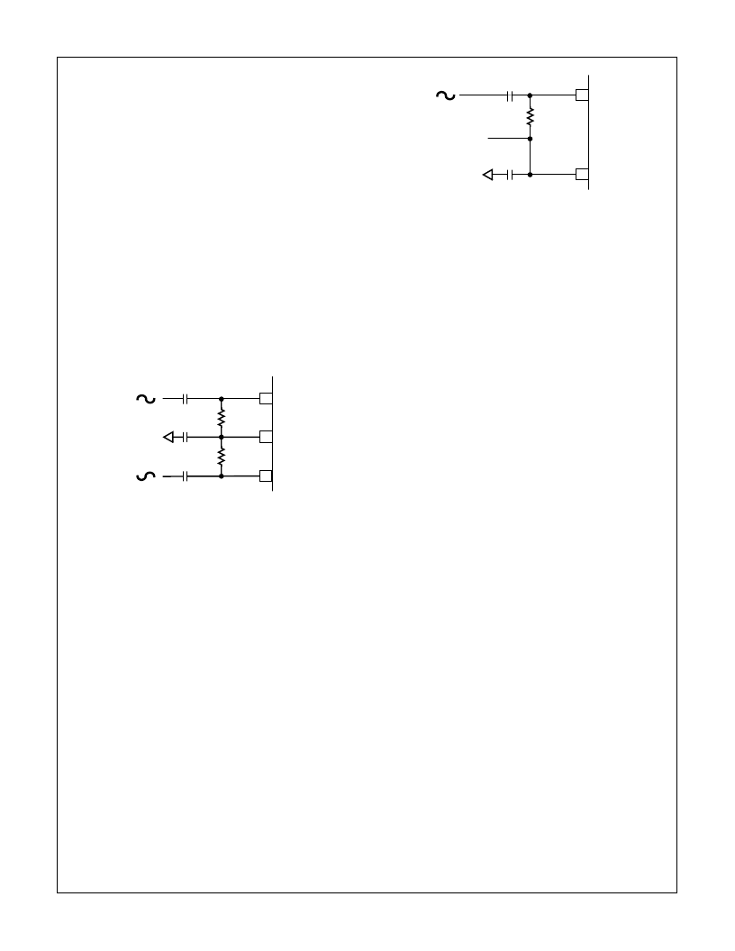
FIGURE 10. AC COUPLED DIFFERENTIAL INPUT
V
IN
+
V
IN
-
HI5804
V
IN
VDC
FIGURE 11. AC COUPLED SINGLE ENDED INPUT
相关PDF资料 |
PDF描述 |
|---|---|
| HI5804EVAL | 12-Bit, 5 MSPS A/D Converter |
| HI5804KCB | 12-Bit, 5 MSPS A/D Converter |
| HI5812JIB | CMOS 20 Microsecond, 12-Bit, Sampling A/D Converter with Internal Track and Hold |
| HI5812JIJ | CMOS 20 Microsecond, 12-Bit, Sampling A/D Converter with Internal Track and Hold |
| HI5812JIP | CMOS 20 Microsecond, 12-Bit, Sampling A/D Converter with Internal Track and Hold |
相关代理商/技术参数 |
参数描述 |
|---|---|
| HI5804EVAL | 制造商:Rochester Electronics LLC 功能描述:- Bulk 制造商:Harris Corporation 功能描述: |
| hi5804kcb | 制造商:Rochester Electronics LLC 功能描述:- Bulk 制造商:Harris Corporation 功能描述: |
| HI5805 | 制造商:INTERSIL 制造商全称:Intersil Corporation 功能描述:12-Bit, 5MSPS A/D Converter |
| HI5805_05 | 制造商:INTERSIL 制造商全称:Intersil Corporation 功能描述:12-Bit, 5MSPS A/D Converter |
| HI5805BIB | 功能描述:IC ADC 12-BIT 5MSPS 28-SOIC RoHS:否 类别:集成电路 (IC) >> 数据采集 - 模数转换器 系列:- 产品培训模块:Lead (SnPb) Finish for COTS Obsolescence Mitigation Program 标准包装:2,500 系列:- 位数:12 采样率(每秒):3M 数据接口:- 转换器数目:- 功率耗散(最大):- 电压电源:- 工作温度:- 安装类型:表面贴装 封装/外壳:SOT-23-6 供应商设备封装:SOT-23-6 包装:带卷 (TR) 输入数目和类型:- |
发布紧急采购,3分钟左右您将得到回复。