参数资料
| 型号: | HI5860IBZ-T |
| 厂商: | Intersil |
| 文件页数: | 6/12页 |
| 文件大小: | 0K |
| 描述: | CONV D/A 12BIT 130MSPS 28-SOIC |
| 标准包装: | 1 |
| 设置时间: | 35ns |
| 位数: | 12 |
| 数据接口: | 并联 |
| 转换器数目: | 1 |
| 电压电源: | 模拟和数字 |
| 功率耗散(最大): | 200mW |
| 工作温度: | -40°C ~ 85°C |
| 安装类型: | 表面贴装 |
| 封装/外壳: | 28-SOIC(0.295",7.50mm 宽) |
| 供应商设备封装: | 28-SOIC W |
| 包装: | 剪切带 (CT) |
| 输出数目和类型: | 2 电流,单极 |
| 采样率(每秒): | 130M |
| 其它名称: | HI5860IBZ-TCT |
3
FN4654.7
February 6, 2008
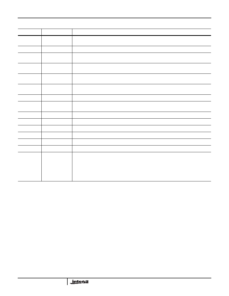
Pin Descriptions
PIN NUMBER
PIN NAME
PIN DESCRIPTION
1 through 12
D11 (MSB) Through
D0 (LSB)
Digital Data Bit 11, (Most Significant Bit) through Digital Data Bit 0, (Least Significant Bit).
13,14
NC
No Connect. (Available as 2 additional LSBs on the HI5960, 14-bit device).
15
SLEEP
Control Pin for Power-Down Mode. Sleep Mode is active high; connect to ground for Normal Mode. Sleep
pin has internal 20
μA active pull-down current.
16
REFLO
Connect to analog ground to enable internal 1.2V reference or connect to AVDD to disable internal
reference.
17
REFIO
Reference voltage input if internal reference is disabled. Reference voltage output if internal reference is
enabled. Use 0.1F cap to ground when internal reference is enabled.
18
FSADJ
Full Scale Current Adjust. Use a resistor to ground to adjust full scale output current. Full Scale Output
Current = 32 x VFSADJ/RSET.
19
COMP1
For use in reducing bandwidth/noise. Recommended: Connect 0.1F to AVDD.
21
IOUTB
The complementary current output of the device. Full scale output current is achieved when all input bits
are set to binary 0.
22
IOUTA
Current output of the device. Full scale output current is achieved when all input bits are set to binary 1.
23
COMP2
Connect 0.1F capacitor to ACOM.
24
AVDD
Analog Supply (+2.7V to +5.5V).
20, 25
ACOM
Connect to Analog Ground.
26
DCOM
Connect to Digital Ground.
27
DVDD
Digital Supply (+2.7V to +5.5V).
28
CLK
Clock Input. Input data to the DAC passes through the “master” latches when the clock is low and is
latched into the “master” latches when the clock is high. Data presented to the “slave” latch passes
through when the clock is logic high and is latched into the “slave” latches when the clock is logic low.
Adequate setup time must be allowed for the MSBs to pass through the thermometer decoder before the
clock goes high. This master-slave arrangement comprises an edge-triggered flip-flop, with the DAC
being updated on the rising clock edge. For optimum spectral performance, it is recommended that the
clock edge be skewed such that set-up time is larger than the hold time.
HI5860
相关PDF资料 |
PDF描述 |
|---|---|
| LT1192CS8#PBF | IC OP-AMP VIDEO HISPD SNGL 8SOIC |
| LT1192CS8 | IC OP-AMP VIDEO HISPD SNGL 8SOIC |
| LT1195CS8#PBF | IC OP-AMP LOW-PWR HI-SPEED 8SOIC |
| 1838894-3 | CONN MALE M12 5POS STR FRONT MT |
| LT1195CS8 | IC OP-AMP LOW-PWR HI-SPEED 8SOIC |
相关代理商/技术参数 |
参数描述 |
|---|---|
| HI5860S0ICEVALI | 制造商:Harris Corporation 功能描述: |
| HI5860SOICEVAL1 | 功能描述:数据转换 IC 开发工具 HI5860 EVAL PL ATFORM PKG RoHS:否 制造商:Texas Instruments 产品:Demonstration Kits 类型:ADC 工具用于评估:ADS130E08 接口类型:SPI 工作电源电压:- 6 V to + 6 V |
| HI5865 | 制造商:INTERSIL 制造商全称:Intersil Corporation 功能描述:12-Bit, 65 MSPS A/D Converter |
| HI5865EVAL1 | 制造商:INTERSIL 制造商全称:Intersil Corporation 功能描述:12-Bit, 65 MSPS A/D Converter |
| HI5865IN | 制造商:INTERSIL 制造商全称:Intersil Corporation 功能描述:12-Bit, 65 MSPS A/D Converter |
发布紧急采购,3分钟左右您将得到回复。