- 您现在的位置:买卖IC网 > PDF目录385381 > HI7190EVAL (Intersil Corporation) null24-Bit, High Precision, Sigma Delta A/D Converter PDF资料下载
参数资料
| 型号: | HI7190EVAL |
| 厂商: | Intersil Corporation |
| 英文描述: | null24-Bit, High Precision, Sigma Delta A/D Converter |
| 中文描述: | null24位,精度高,Σ-ΔA / D转换 |
| 文件页数: | 15/24页 |
| 文件大小: | 187K |
| 代理商: | HI7190EVAL |
1885
It is important to realize that the user can interrupt a data
transfer on byte boundaries. That is, if the Instruction Regis-
ter calls for a 3 byte transfer and CS is inactive after only one
byte has been transferred, the HI7190, when reactivated, will
continue with the remaining two bytes before looking for the
next Instruction Register write cycle.
Note that the outputs will NOT go three-state immediately upon
CS inactive for read operations in self-clocking mode. In the
case of CS going inactive during a read cycle the outputs
remain driving until after the last data bit is transferred. In the
case of CS inactive during the clock stall time it takes 1 OSC
1
cycle plus prop delay (Max) for the outputs to be disabled.
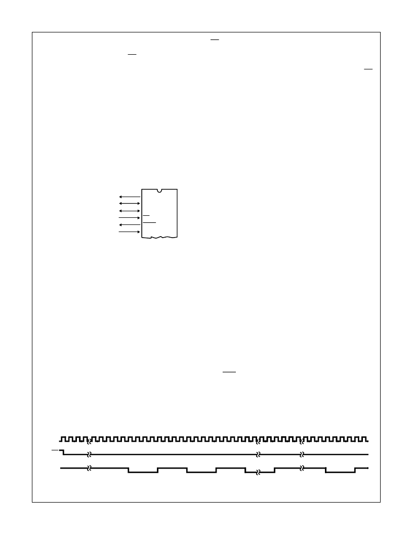
I/O Port Pin Descriptions
The serial I/O port is a bidirectional port which is used to
read the data register and read or write the control register
and calibration registers. The port contains two data lines, a
synchronous clock, and a status flag. Figure 12 shows a
diagram of the serial interface lines.
SDO
- Serial Data out. Data is read from this line using those
protocols with separate lines for transmitting and receiving
data. An example of such a standard is the Motorola Serial
Peripheral Interface (SPI) using the 68HC05 and 68HC11
family of microcontrollers, or other similar processors. In the
case of using bidirectional data transfer on SDIO, SDO does
not output data and is set in a high impedance state.
SDIO
- Serial Data in or out. Data is always written to the
device on this line. However, this line can be used as a bidi-
rectional data line. This is done by properly setting up the
Control Register. Bidirectional data transfer on this line can
be used with Intel standard serial interfaces (SSR, Mode 0)
in MCS51 and MCS96 family of microcontrollers, or other
similar processors.
SCLK
- Serial clock. The serial clock pin is used to synchro-
nize data to and from the HI7190 and to run the port state
machines. In Synchronous External Clock Mode, SCLK is
configured as an input, is supplied by the user, and can run
up to a 5MHz rate. In Synchronous Self Clocking Mode,
SCLK is configured as an output and runs at OSC
1
/8.
CS
- Chip select. This signal is an active low input that
allows more than one device on the same serial communica-
tion lines. The SDO and SDIO will go to a high impedance
state when this signal is high. If driven high during any
communication cycle, that cycle will be suspended until CS
reactivation. Chip select can be tied low in systems that
maintain control of SCLK.
DRDY
- Data Ready. This is an output status flag from the
device to signal that the Data Output Register has been
updated with the new conversion result. DRDY is useful as an
edge or level sensitive interrupt signal to a microprocessor or
microcontroller. DRDY low indicates that new data is available
at the Data Output Register. DRDY will return high upon
completion of a complete Data Output Register read cycle.
MODE
- Mode. This input is used to select between Synchro-
nous Self Clocking Mode (‘1’) or the Synchronous External
Clocking Mode (‘0’). When this pin is tied to V
DD
the serial
port is configured in the Synchronous Self Clocking mode
where the synchronous shift clock (SCLK) for the serial port is
generated by the HI7190 and has a frequency of OSC
1
/8.
When the pin is tied to DGND the serial port is configured for
the Synchronous External Clocking Mode where the synchro-
nous shift clock for the serial port is generated by an external
device up to a maximum frequency of 5MHz.
Programming the Serial Interface
It is useful to think of the HI7190 interface in terms of
communication cycles. Each communication cycle happens
in 2 phases. The first phase of every communication cycle
is the writing of an instruction byte. The second phase is
the data transfer as described by the instruction byte. It is
important to note that phase 2 of the communication cycle
can be a single byte or a multi-byte transfer of data. For
example, the 3-byte Data Output Register can be read
using one multi-byte communication cycle rather than three
single-byte communication cycles. It is up to the user to
maintain synchronism with respect to data transfers. If the
system processor “gets lost” the only way to recover is to
reset the HI7190. Figure 14 shows both a 2-wire and a
3-wire data transfer.
Several formats are available for reading from and writing to
the HI7190 registers in both the 2-wire and 3-wire protocols.
A portion of these formats is controlled by the CR<2:1> (BD
and MSB) bits which control the byte direction and bit order
of a data transfer respectively. These two bits can be written
in any combination but only the two most useful will be dis-
cussed here.
CHIP SELECT
DEVICE STATUS
CLOCK MODE
SDO
SDIO
SCLK
CS
DRDY
MODE
HI7190
BIDIRECTIONAL DATA
PORT CLOCK
DATA OUT
FIGURE 11. HI7190 SERIAL INTERFACE
OSC
1
CS
SCLK
29
33
37
41
45
89
121
125
FIGURE 12. SCLK OUTPUT IN SELF-CLOCKING MODE
HI7190
相关PDF资料 |
PDF描述 |
|---|---|
| HI7190IB | null24-Bit, High Precision, Sigma Delta A/D Converter |
| HIH-3602-A | Humidity Sensor(湿度传感器) |
| HIH-3602-L-CP | Humidity Sensor(湿度传感器) |
| HIN240 | 5V High-Speed RS-232 Transceivers with 0.1uF Capacitors |
| HIN240CN | 5V High-Speed RS-232 Transceivers with 0.1uF Capacitors |
相关代理商/技术参数 |
参数描述 |
|---|---|
| HI7190IB | 功能描述:IC ADC 24BIT PROGBL SER 20-SOIC RoHS:否 类别:集成电路 (IC) >> 数据采集 - 模数转换器 系列:- 产品培训模块:Lead (SnPb) Finish for COTS Obsolescence Mitigation Program 标准包装:2,500 系列:- 位数:12 采样率(每秒):3M 数据接口:- 转换器数目:- 功率耗散(最大):- 电压电源:- 工作温度:- 安装类型:表面贴装 封装/外壳:SOT-23-6 供应商设备封装:SOT-23-6 包装:带卷 (TR) 输入数目和类型:- |
| HI7190IBZ | 功能描述:模数转换器 - ADC ADC 24BIT 10MHZ SIGMADELTA 20 IND RoHS:否 制造商:Texas Instruments 通道数量:2 结构:Sigma-Delta 转换速率:125 SPs to 8 KSPs 分辨率:24 bit 输入类型:Differential 信噪比:107 dB 接口类型:SPI 工作电源电压:1.7 V to 3.6 V, 2.7 V to 5.25 V 最大工作温度:+ 85 C 安装风格:SMD/SMT 封装 / 箱体:VQFN-32 |
| HI7190IBZ-T | 功能描述:模数转换器 - ADC ADC 24BIT 10MHZ SIGMADELTA 20 IND RoHS:否 制造商:Texas Instruments 通道数量:2 结构:Sigma-Delta 转换速率:125 SPs to 8 KSPs 分辨率:24 bit 输入类型:Differential 信噪比:107 dB 接口类型:SPI 工作电源电压:1.7 V to 3.6 V, 2.7 V to 5.25 V 最大工作温度:+ 85 C 安装风格:SMD/SMT 封装 / 箱体:VQFN-32 |
| HI7190IP | 功能描述:IC ADC 24BIT PROGBL SER 20-PDIP RoHS:否 类别:集成电路 (IC) >> 数据采集 - 模数转换器 系列:- 产品培训模块:Lead (SnPb) Finish for COTS Obsolescence Mitigation Program 标准包装:2,500 系列:- 位数:12 采样率(每秒):3M 数据接口:- 转换器数目:- 功率耗散(最大):- 电压电源:- 工作温度:- 安装类型:表面贴装 封装/外壳:SOT-23-6 供应商设备封装:SOT-23-6 包装:带卷 (TR) 输入数目和类型:- |
| HI7190IPZ | 功能描述:模数转换器 - ADC W/ANNEAL ADC 24BIT 1 0HZ SIGMADELTA RoHS:否 制造商:Texas Instruments 通道数量:2 结构:Sigma-Delta 转换速率:125 SPs to 8 KSPs 分辨率:24 bit 输入类型:Differential 信噪比:107 dB 接口类型:SPI 工作电源电压:1.7 V to 3.6 V, 2.7 V to 5.25 V 最大工作温度:+ 85 C 安装风格:SMD/SMT 封装 / 箱体:VQFN-32 |
发布紧急采购,3分钟左右您将得到回复。