- 您现在的位置:买卖IC网 > PDF目录385381 > HI7190EVAL (Intersil Corporation) null24-Bit, High Precision, Sigma Delta A/D Converter PDF资料下载
参数资料
| 型号: | HI7190EVAL |
| 厂商: | Intersil Corporation |
| 英文描述: | null24-Bit, High Precision, Sigma Delta A/D Converter |
| 中文描述: | null24位,精度高,Σ-ΔA / D转换 |
| 文件页数: | 9/24页 |
| 文件大小: | 187K |
| 代理商: | HI7190EVAL |
1879
or self-calibration where only the HI7190 itself is in the cali-
bration loop. The On-chip Calibration Registers are
read/write registers which allow the user to read calibration
coefficients as well as write previously determined
calibration coefficients.
Circuit Operation
The analog and digital supplies and grounds are separate
on the HI7190 to minimize digital noise coupling into the
analog circuitry. Nominal supply voltages are AV
DD
= +5V,
DV
DD
= +5V, and AV
SS
= -5V. If the same supply is used
for AV
DD
and DV
DD
it is imperative that the supply is sepa-
rately decoupled to the AV
DD
and DV
DD
pins on the
HI7190. Separate analog and digital ground planes should
be maintained on the system board and the grounds should
be tied together back at the power supply.
When the HI7190 is powered up it needs to be reset by pull-
ing the RESET line low. The reset sets the internal registers
of the HI7190 as shown in Table 2 and puts the part in the
bipolar mode with a gain of 1 and offset binary coding. The
filter notch of the digital filter is set at 30Hz while the I/O is
set up for bidirectional I/O (data is read and written on the
SDIO line and SDO is three-stated), descending byte order,
and MSB first data format. A self calibration is performed
before the device begins converting. DRDY goes low when
valid data is available at the output.
The configuration of the HI7190 is changed by writing new
setup data to the Control Register. Whenever data is written
to byte 2 and/or byte 1 of the Control Register the part
assumes that a critical setup parameter is being changed
which means that DRDY goes high and the device is re-syn-
chronized. If the configuration is changed such that the
device is in any one of the calibration modes, a new calibra-
tion is performed before normal conversions continue. If the
device is written to the conversion mode, a new calibration is
NOT performed (A new calibration is recommended any time
data is written to the Control Register.). In either case, DRDY
goes low when valid data is available at the output.
If a single data byte is written to byte 0 of the Control
Register, the device assumes the gain has NOT been
changed. It is up to the user to re-calibrate the device if the
gain is changed in this manner. For this reason it is
recommended that the entire Control Register be written
when changing the gain of the device. This ensures that the
part is re-calibrated (if in a calibration mode) before the
DRDY output goes low indicating that valid data is available.
The calibration registers can be read via the serial interface
at any time. However, care must be taken when writing data
to the calibration registers. If the HI7190 is internally
updating any calibration register the user can not write to
that calibration register. See the Operational Modes section
for details on which calibration registers are updated for the
various modes.
Since access to the calibration registers is asynchronous to
the conversion process the user is cautioned that new
calibration data may not be used on the very next set of
“valid” data after a calibration register write. It is guaranteed
that the new data will take effect on the second set of output
data. Non-calibrated data can be obtained from the device
by writing 000000 (h) to the Offset Calibration Register,
800000 (h) to the Positive Full Scale Calibration Register,
and 800000 (h) to the Negative Full Scale Calibration Regis-
ter. This sets the offset correction factor to 0 and the positive
and negative gain slope factors to 1.
If several HI7190s share a system master clock the
SYNC
pin can be used to synchronize their operation. A common
SYNC
input to multiple devices will synchronize operation
such that all output registers are updated simultaneously. Of
course the
SYNC
pin would normally be activated only after
each HI7190 has been calibrated or has had calibration
coefficients written to it.
The
SYNC
pin can also be used to control the HI7190 when
an external multiplexer is used with a single HI7190. The
SYNC
pin in this application can be used to guarantee a max-
imum settling time of 3 conversion periods when switching
channels on the multiplexer.
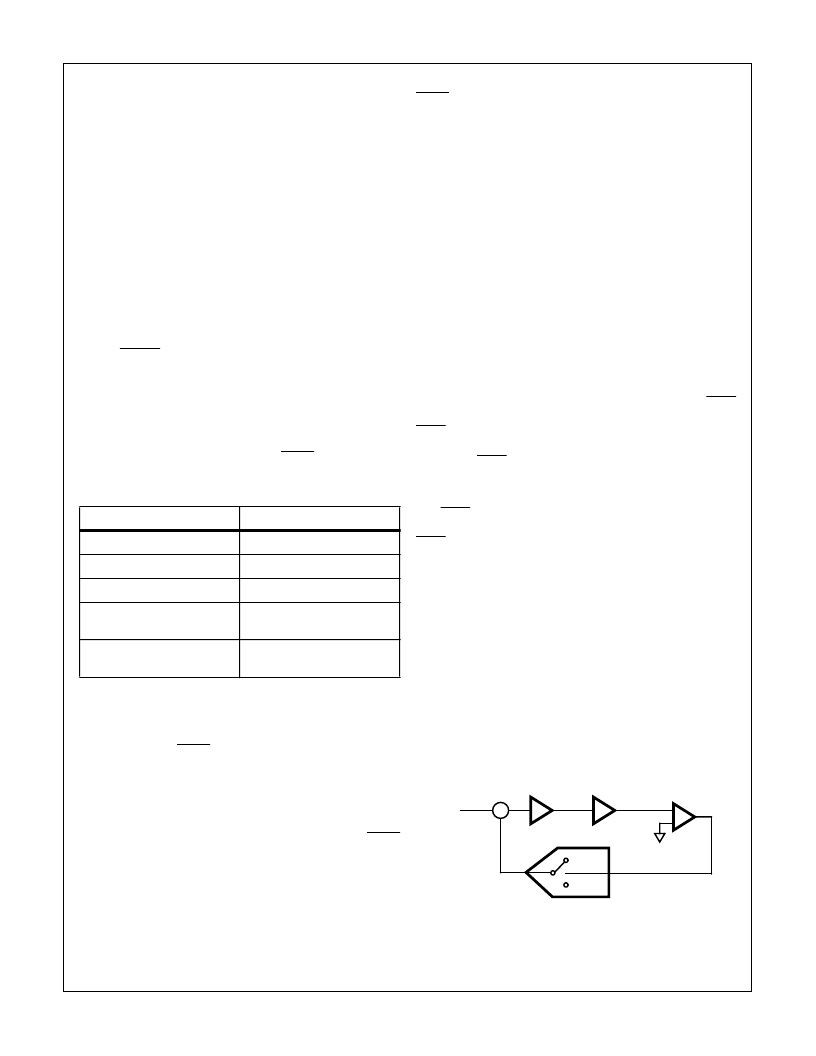
Analog Section Description
Figure 6 shows a simplified block diagram of the analog
modulator front end of a sigma delta A/D Converter. The
input signal V
IN
comes into a summing junction (the PGIA in
this case) where the previous modulator output is subtracted
from it. The resulting signal is then integrated and the output
of the integrator goes into the comparator. The output of the
comparator is then fed back via a 1-bit DAC to the summing
junction. The feedback loop forces the average of the fed
back signal to be equal to the input signal V
IN
.
TABLE 2. REGISTER RESET VALUES
REGISTER
VALUE (HEX)
Data Output Register
XXXX (Undefined)
Control Register
28B300
Offset Calibration Register
Self Calibration Value
Positive Full Scale Calibration
Register
Self Calibration Value
Negative Full Scale Calibration
Register
Self Calibration Value
PGIA
INTEGRATOR
COMPARATOR
V
RHI
V
RLO
DAC
V
IN
+
-
∫
∑
+
-
FIGURE 6. SIMPLE MODULATOR BLOCK DIAGRAM
HI7190
相关PDF资料 |
PDF描述 |
|---|---|
| HI7190IB | null24-Bit, High Precision, Sigma Delta A/D Converter |
| HIH-3602-A | Humidity Sensor(湿度传感器) |
| HIH-3602-L-CP | Humidity Sensor(湿度传感器) |
| HIN240 | 5V High-Speed RS-232 Transceivers with 0.1uF Capacitors |
| HIN240CN | 5V High-Speed RS-232 Transceivers with 0.1uF Capacitors |
相关代理商/技术参数 |
参数描述 |
|---|---|
| HI7190IB | 功能描述:IC ADC 24BIT PROGBL SER 20-SOIC RoHS:否 类别:集成电路 (IC) >> 数据采集 - 模数转换器 系列:- 产品培训模块:Lead (SnPb) Finish for COTS Obsolescence Mitigation Program 标准包装:2,500 系列:- 位数:12 采样率(每秒):3M 数据接口:- 转换器数目:- 功率耗散(最大):- 电压电源:- 工作温度:- 安装类型:表面贴装 封装/外壳:SOT-23-6 供应商设备封装:SOT-23-6 包装:带卷 (TR) 输入数目和类型:- |
| HI7190IBZ | 功能描述:模数转换器 - ADC ADC 24BIT 10MHZ SIGMADELTA 20 IND RoHS:否 制造商:Texas Instruments 通道数量:2 结构:Sigma-Delta 转换速率:125 SPs to 8 KSPs 分辨率:24 bit 输入类型:Differential 信噪比:107 dB 接口类型:SPI 工作电源电压:1.7 V to 3.6 V, 2.7 V to 5.25 V 最大工作温度:+ 85 C 安装风格:SMD/SMT 封装 / 箱体:VQFN-32 |
| HI7190IBZ-T | 功能描述:模数转换器 - ADC ADC 24BIT 10MHZ SIGMADELTA 20 IND RoHS:否 制造商:Texas Instruments 通道数量:2 结构:Sigma-Delta 转换速率:125 SPs to 8 KSPs 分辨率:24 bit 输入类型:Differential 信噪比:107 dB 接口类型:SPI 工作电源电压:1.7 V to 3.6 V, 2.7 V to 5.25 V 最大工作温度:+ 85 C 安装风格:SMD/SMT 封装 / 箱体:VQFN-32 |
| HI7190IP | 功能描述:IC ADC 24BIT PROGBL SER 20-PDIP RoHS:否 类别:集成电路 (IC) >> 数据采集 - 模数转换器 系列:- 产品培训模块:Lead (SnPb) Finish for COTS Obsolescence Mitigation Program 标准包装:2,500 系列:- 位数:12 采样率(每秒):3M 数据接口:- 转换器数目:- 功率耗散(最大):- 电压电源:- 工作温度:- 安装类型:表面贴装 封装/外壳:SOT-23-6 供应商设备封装:SOT-23-6 包装:带卷 (TR) 输入数目和类型:- |
| HI7190IPZ | 功能描述:模数转换器 - ADC W/ANNEAL ADC 24BIT 1 0HZ SIGMADELTA RoHS:否 制造商:Texas Instruments 通道数量:2 结构:Sigma-Delta 转换速率:125 SPs to 8 KSPs 分辨率:24 bit 输入类型:Differential 信噪比:107 dB 接口类型:SPI 工作电源电压:1.7 V to 3.6 V, 2.7 V to 5.25 V 最大工作温度:+ 85 C 安装风格:SMD/SMT 封装 / 箱体:VQFN-32 |
发布紧急采购,3分钟左右您将得到回复。