参数资料
| 型号: | HIP6004BCB-T |
| 厂商: | Intersil |
| 文件页数: | 11/15页 |
| 文件大小: | 0K |
| 描述: | IC CTRLR PWM VOLTAGE MON 20-SOIC |
| 标准包装: | 1,000 |
| 应用: | 控制器,Intel Pentium?,II,Pro |
| 输入电压: | 5V,12V |
| 输出数: | 1 |
| 输出电压: | 1.3 V ~ 3.5 V |
| 工作温度: | 0°C ~ 70°C |
| 安装类型: | 表面贴装 |
| 封装/外壳: | 20-SOIC(0.295",7.50mm 宽) |
| 供应商设备封装: | 20-SOIC W |
| 包装: | 带卷 (TR) |
�� �
�
�HIP6004B�
�below).� Only� the� upper� MOSFET� has� switching� losses,� since�
�the� Schottky� rectifier� clamps� the� switching� node� before� the�
�synchronous� rectifier� turns� on.� These� equations� assume� linear�
�voltage-current� transitions� and� do� not� adequately� model� power�
�loss� due� the� reverse-recovery� of� the� lower� MOSFET’s� body�
�diode.� The� gate-charge� losses� are� dissipated� by� the� HIP6004B�
�and� don't� heat� the� MOSFETs.� However,� large� gate-charge�
�increases� the� switching� interval,� t� SW� which� increases� the� upper�
�MOSFET� switching� losses.� Ensure� that� both� MOSFETs� are�
�within� their� maximum� junction� temperature� at� high� ambient�
�temperature� by� calculating� the� temperature� rise� according� to�
�package� thermal-resistance� specifications.� A� separate� heatsink�
�may� be� necessary� depending� upon� MOSFET� power,� package�
�type,� ambient� temperature� and� air� flow.�
�Figure� 10� shows� the� upper� gate� drive� supplied� by� a� direct�
�connection� to� V� CC� .� This� option� should� only� be� used� in�
�converter� systems� where� the� main� input� voltage� is� +5V� DC� or�
�less.� The� peak� upper� gate-to-source� voltage� is� approximately�
�V� CC� less� the� input� supply.� For� +5V� main� power� and� +12V� DC�
�for� the� bias,� the� gate-to-source� voltage� of� Q� 1� is� 7V.� A� logic-�
�level� MOSFET� is� a� good� choice� for� Q� 1� and� a� logic-level�
�MOSFET� can� be� used� for� Q� 2� if� its� absolute� gate-to-source�
�voltage� rating� exceeds� the� maximum� voltage� applied� to� V� CC� .�
�+12V�
�+5V� OR� LESS�
�V� CC�
�P� UPPER� =� Io� 2� x� r� DS(ON)� x� D� +�
�1�
�2�
�Io� x� V� IN� x� t� SW� x� F� S�
�HIP6004B�
�BOOT�
�P� LOWER� =� Io� 2� x� r� DS(ON)� x� (1� -� D)�
�Where:� D� is� the� duty� cycle� =� V� OUT� /� V� IN� ,�
�t� SW� is� the� switch� ON� time,� and�
�UGATE�
�PHASE�
�Q� 1�
�NOTE:�
�V� G-S� ≈� V� CC� -5V�
�F� S� is� the� switching� frequency.�
�Standard-gate� MOSFETs� are� normally� recommended� for�
�use� with� the� HIP6004B.� However,� logic-level� gate� MOSFETs�
�can� be� used� under� special� circumstances.� The� input� voltage,�
�-�
�+�
�LGATE�
�PGND�
�GND�
�Q� 2�
�D� 2�
�NOTE:�
�V� G-S� ≈� V� CC�
�upper� gate� drive� level,� and� the� MOSFET’s� absolute� gate-to-�
�source� voltage� rating� determine� whether� logic-level�
�MOSFETs� are� appropriate.�
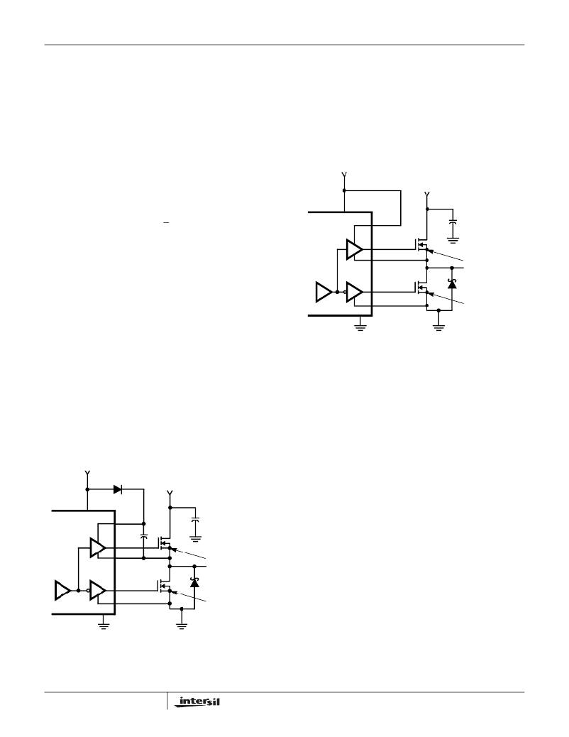
�Figure� 9� shows� the� upper� gate� drive� (BOOT� pin)� supplied� by� a�
�bootstrap� circuit� from� V� CC� .� The� boot� capacitor,� C� BOOT�
�develops� a� floating� supply� voltage� referenced� to� the� PHASE�
�pin.� This� supply� is� refreshed� each� cycle� to� a� voltage� of� V� CC�
�less� the� boot� diode� drop� (V� D� )� when� the� lower� MOSFET,� Q� 2�
�turns� on.� Logic-level� MOSFETs� can� only� be� used� if� the�
�MOSFET’s� absolute� gate-to-source� voltage� rating� exceeds�
�the� maximum� voltage� applied� to� V� CC� .�
�+12V�
�D� BOOT�
�FIGURE� 10.� UPPER� GATE� DRIVE� -� DIRECT� V� CC� DRIVE� OPTION�
�Schottky� Selection�
�Rectifier� D� 2� is� a� clamp� that� catches� the� negative� inductor�
�swing� during� the� dead� time� between� turning� off� the� lower�
�MOSFET� and� turning� on� the� upper� MOSFET.� The� diode�
�must� be� a� Schottky� type� to� prevent� the� lossy� parasitic�
�MOSFET� body� diode� from� conducting.� It� is� acceptable� to�
�omit� the� diode� and� let� the� body� diode� of� the� lower� MOSFET�
�clamp� the� negative� inductor� swing,� but� efficiency� will� drop�
�one� or� two� percent� as� a� result.� The� diode’s� rated� reverse�
�breakdown� voltage� must� be� greater� than� the� maximum�
�input� voltage.�
�V� CC�
�HIP6004B�
�+� V� D� -�
�BOOT�
�UGATE�
�PHASE�
�C� BOOT�
�+5V� OR� +12V�
�Q1�
�NOTE:�
�V� G-S� ≈� V� CC� -V� D�
�-�
�+�
�LGATE�
�PGND�
�Q2�
�D2�
�NOTE:�
�V� G-S� ≈� V� CC�
�GND�
�FIGURE� 9.� UPPER� GATE� DRIVE� -� BOOTSTRAP� OPTION�
�11�
�相关PDF资料 |
PDF描述 |
|---|---|
| UVK2V4R7MPD | CAP ALUM 4.7UF 350V 20% RADIAL |
| UVK1V331MPD | CAP ALUM 330UF 35V 20% RADIAL |
| EL7585ILZ | IC POWER SUPPLY TFT-LCD 20-QFN |
| EL7585AILZ-T13 | IC POWER SUPPLY TFT-LCD 20-QFN |
| HSM24DRXH | CONN EDGECARD 48POS DIP .156 SLD |
相关代理商/技术参数 |
参数描述 |
|---|---|
| HIP6004BCBZ | 功能描述:电压模式 PWM 控制器 PWM CNTRLR 3 5 TO 1 3 DAC RNG 20LD RoHS:否 制造商:Texas Instruments 输出端数量:1 拓扑结构:Buck 输出电压:34 V 输出电流: 开关频率: 工作电源电压:4.5 V to 5.5 V 电源电流:600 uA 最大工作温度:+ 125 C 最小工作温度:- 40 C 封装 / 箱体:WSON-8 封装:Reel |
| HIP6004BCBZA | 功能描述:电压模式 PWM 控制器 W/ANNEAL PWM CNTRLR 3 5 TO 1 3 DAC RNG RoHS:否 制造商:Texas Instruments 输出端数量:1 拓扑结构:Buck 输出电压:34 V 输出电流: 开关频率: 工作电源电压:4.5 V to 5.5 V 电源电流:600 uA 最大工作温度:+ 125 C 最小工作温度:- 40 C 封装 / 箱体:WSON-8 封装:Reel |
| HIP6004BCBZA-T | 功能描述:电压模式 PWM 控制器 W/ANNEAL PWM CNTRLR 3 5V TO 1 3V DAC RoHS:否 制造商:Texas Instruments 输出端数量:1 拓扑结构:Buck 输出电压:34 V 输出电流: 开关频率: 工作电源电压:4.5 V to 5.5 V 电源电流:600 uA 最大工作温度:+ 125 C 最小工作温度:- 40 C 封装 / 箱体:WSON-8 封装:Reel |
| HIP6004BCBZ-T | 功能描述:电压模式 PWM 控制器 PWM CNTRLR 3 5V TO 1 3V DAC 20LD TA RoHS:否 制造商:Texas Instruments 输出端数量:1 拓扑结构:Buck 输出电压:34 V 输出电流: 开关频率: 工作电源电压:4.5 V to 5.5 V 电源电流:600 uA 最大工作温度:+ 125 C 最小工作温度:- 40 C 封装 / 箱体:WSON-8 封装:Reel |
| HIP6004BCR | 功能描述:IC CTRLR PWM VOLTAGE MON 20-QFN RoHS:否 类别:集成电路 (IC) >> PMIC - 稳压器 - 专用型 系列:- 产品培训模块:Lead (SnPb) Finish for COTS Obsolescence Mitigation Program 标准包装:2,000 系列:- 应用:电源,ICERA E400,E450 输入电压:4.1 V ~ 5.5 V 输出数:10 输出电压:可编程 工作温度:-40°C ~ 85°C 安装类型:表面贴装 封装/外壳:42-WFBGA,WLCSP 供应商设备封装:42-WLP 包装:带卷 (TR) |
发布紧急采购,3分钟左右您将得到回复。