参数资料
| 型号: | HIP6004BCB-T |
| 厂商: | Intersil |
| 文件页数: | 7/15页 |
| 文件大小: | 0K |
| 描述: | IC CTRLR PWM VOLTAGE MON 20-SOIC |
| 标准包装: | 1,000 |
| 应用: | 控制器,Intel Pentium?,II,Pro |
| 输入电压: | 5V,12V |
| 输出数: | 1 |
| 输出电压: | 1.3 V ~ 3.5 V |
| 工作温度: | 0°C ~ 70°C |
| 安装类型: | 表面贴装 |
| 封装/外壳: | 20-SOIC(0.295",7.50mm 宽) |
| 供应商设备封装: | 20-SOIC W |
| 包装: | 带卷 (TR) |
�� �
�
�HIP6004B�
�I� PEAK� =� -----------------------------------------------------�
�Over-Current� Protection�
�The� over-current� function� protects� the� converter� from� a�
�shorted� output� by� using� the� upper� MOSFET’s� on-resistance,�
�r� DS(ON)� to� monitor� the� current.� This� method� enhances� the�
�converter’s� efficiency� and� reduces� cost� by� eliminating� a�
�current� sensing� resistor.�
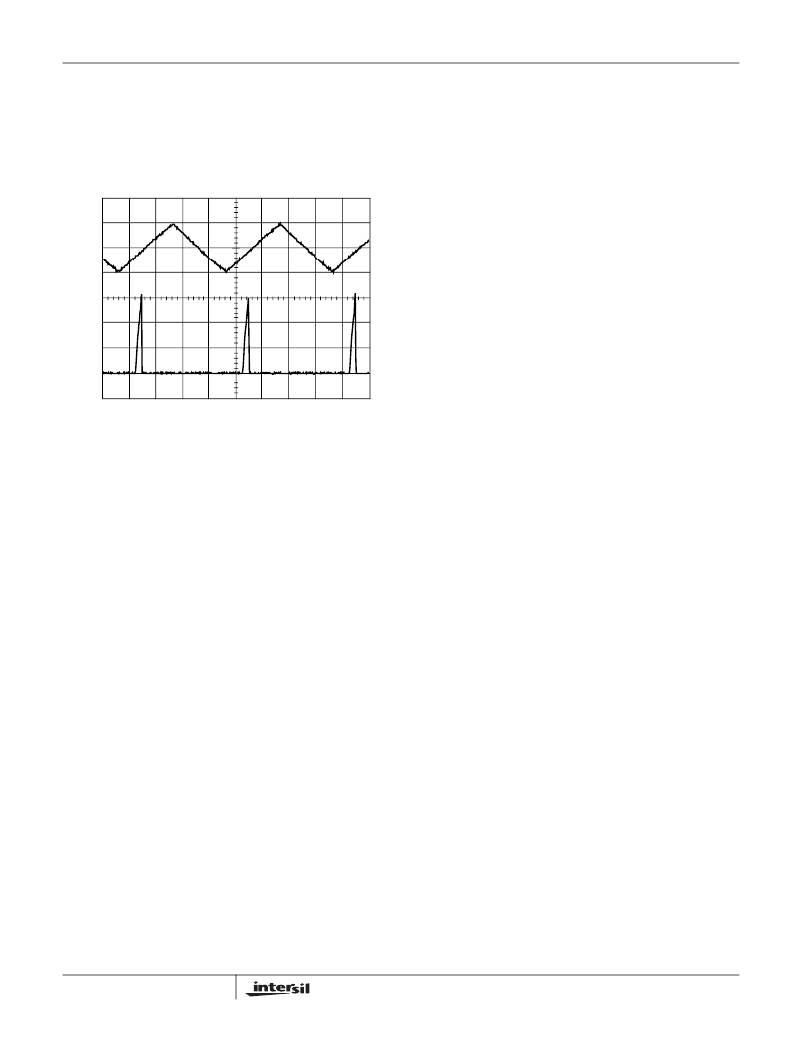
�4V�
�2V�
�0V�
�15A�
�10A�
�5A�
�0A�
�TIME� (20ms/DIV)�
�FIGURE� 4.� OVER-CURRENT� OPERATION�
�The� over-current� function� cycles� the� soft-start� function� in� a�
�hiccup� mode� to� provide� fault� protection.� A� resistor� (R� OCSET� )�
�programs� the� over-current� trip� level.� An� internal� 200μA� current�
�sink� develops� a� voltage� across� R� OCSET� that� is� referenced� to�
�V� IN� .� When� the� voltage� across� the� upper� MOSFET� (also�
�referenced� to� V� IN� )� exceeds� the� voltage� across� R� OCSET� ,� the�
�over-current� function� initiates� a� soft-start� sequence.� The� soft-�
�start� function� discharges� C� SS� with� a� 10μA� current� sink� and�
�inhibits� PWM� operation.� The� soft-start� function� recharges�
�C� SS� ,� and� PWM� operation� resumes� with� the� error� amplifier�
�clamped� to� the� SS� voltage.� Should� an� overload� occur� while�
�recharging� C� SS� ,� the� soft� start� function� inhibits� PWM� operation�
�while� fully� charging� C� SS� to� 4V� to� complete� its� cycle.� Figure� 4�
�shows� this� operation� with� an� overload� condition.� Note� that� the�
�inductor� current� increases� to� over� 15A� during� the� C� SS�
�charging� interval� and� causes� an� over-current� trip.� The�
�converter� dissipates� very� little� power� with� this� method.� The�
�measured� input� power� for� the� conditions� of� Figure� 4� is� 2.5W.�
�The� over-current� function� will� trip� at� a� peak� inductor� current�
�(I� PEAK)� determined� by:�
�I� OCSET� x� R� OCSET�
�r� DS� (� ON� )�
�where� I� OCSET� is� the� internal� OCSET� current� source� (200� μ� A�
�typical).� The� OC� trip� point� varies� mainly� due� to� the�
�MOSFET’s� r� DS(ON)� variations.� To� avoid� over-current�
�tripping� in� the� normal� operating� load� range,� find� the� R� OCSET�
�resistor� from� the� equation� above� with:�
�1.� The� maximum� r� DS(ON)� at� the� highest� junction�
�temperature.�
�2.� The� minimum� I� OCSET� from� the� specification� table.�
�3.� Determine� I� PEAK� for� I� PEAK� >� I� OUT� (� MAX� )� +� (� ?� I� )� ?� 2� ,�
�where� ?� I� is� the� output� inductor� ripple� current.�
�For� an� equation� for� the� ripple� current� see� the� section� under�
�component� guidelines� titled� ‘Output� Inductor� Selection’.�
�A� small� ceramic� capacitor� should� be� placed� in� parallel� with�
�R� OCSET� to� smooth� the� voltage� across� R� OCSET� in� the�
�presence� of� switching� noise� on� the� input� voltage.�
�Output� Voltage� Program�
�The� output� voltage� of� a� HIP6004B� converter� is� programmed�
�to� discrete� levels� between� 1.8V� DC� and� 3.5V� DC� .� The� voltage�
�identification� (VID)� pins� program� an� internal� voltage� reference�
�(DACOUT)� with� a� TTL-compatible� 5-bit� digital-to-analog�
�converter� (DAC).� The� level� of� DACOUT� also� sets� the� PGOOD�
�and� OVP� thresholds.� Table� 1� specifies� the� DACOUT� voltage�
�for� the� 32� different� combinations� of� connections� on� the� VID�
�pins.� The� output� voltage� should� not� be� adjusted� while� the�
�converter� is� delivering� power.� Remove� input� power� before�
�changing� the� output� voltage.� Adjusting� the� output� voltage�
�during� operation� could� toggle� the� PGOOD� signal� and� exercise�
�the� overvoltage� protection.�
�‘11111’� VID� pin� combination� resulting� in� a� 0V� output� setting�
�activates� the� Power-On� Reset� function� and� disables� the� gate�
�drives� circuitry.� For� this� specific� VID� combination,� though,�
�PGOOD� asserts� a� high� level.� This� unusual� behavior� has� been�
�implemented� in� order� to� allow� for� operation� in� dual-�
�microprocessor� systems� where� AND-ing� of� the� PGOOD� signals�
�from� two� individual� power� converters� is� implemented.�
�Application� Guidelines�
�Layout� Considerations�
�As� in� any� high� frequency� switching� converter,� layout� is� very�
�important.� Switching� current� from� one� power� device� to� another�
�can� generate� voltage� transients� across� the� impedances� of� the�
�interconnecting� bond� wires� and� circuit� traces.� These�
�interconnecting� impedances� should� be� minimized� by� using�
�wide,� short� printed� circuit� traces.� The� critical� components�
�should� be� located� as� close� together� as� possible,� using� ground�
�plane� construction� or� single� point� grounding.�
�7�
�相关PDF资料 |
PDF描述 |
|---|---|
| UVK2V4R7MPD | CAP ALUM 4.7UF 350V 20% RADIAL |
| UVK1V331MPD | CAP ALUM 330UF 35V 20% RADIAL |
| EL7585ILZ | IC POWER SUPPLY TFT-LCD 20-QFN |
| EL7585AILZ-T13 | IC POWER SUPPLY TFT-LCD 20-QFN |
| HSM24DRXH | CONN EDGECARD 48POS DIP .156 SLD |
相关代理商/技术参数 |
参数描述 |
|---|---|
| HIP6004BCBZ | 功能描述:电压模式 PWM 控制器 PWM CNTRLR 3 5 TO 1 3 DAC RNG 20LD RoHS:否 制造商:Texas Instruments 输出端数量:1 拓扑结构:Buck 输出电压:34 V 输出电流: 开关频率: 工作电源电压:4.5 V to 5.5 V 电源电流:600 uA 最大工作温度:+ 125 C 最小工作温度:- 40 C 封装 / 箱体:WSON-8 封装:Reel |
| HIP6004BCBZA | 功能描述:电压模式 PWM 控制器 W/ANNEAL PWM CNTRLR 3 5 TO 1 3 DAC RNG RoHS:否 制造商:Texas Instruments 输出端数量:1 拓扑结构:Buck 输出电压:34 V 输出电流: 开关频率: 工作电源电压:4.5 V to 5.5 V 电源电流:600 uA 最大工作温度:+ 125 C 最小工作温度:- 40 C 封装 / 箱体:WSON-8 封装:Reel |
| HIP6004BCBZA-T | 功能描述:电压模式 PWM 控制器 W/ANNEAL PWM CNTRLR 3 5V TO 1 3V DAC RoHS:否 制造商:Texas Instruments 输出端数量:1 拓扑结构:Buck 输出电压:34 V 输出电流: 开关频率: 工作电源电压:4.5 V to 5.5 V 电源电流:600 uA 最大工作温度:+ 125 C 最小工作温度:- 40 C 封装 / 箱体:WSON-8 封装:Reel |
| HIP6004BCBZ-T | 功能描述:电压模式 PWM 控制器 PWM CNTRLR 3 5V TO 1 3V DAC 20LD TA RoHS:否 制造商:Texas Instruments 输出端数量:1 拓扑结构:Buck 输出电压:34 V 输出电流: 开关频率: 工作电源电压:4.5 V to 5.5 V 电源电流:600 uA 最大工作温度:+ 125 C 最小工作温度:- 40 C 封装 / 箱体:WSON-8 封装:Reel |
| HIP6004BCR | 功能描述:IC CTRLR PWM VOLTAGE MON 20-QFN RoHS:否 类别:集成电路 (IC) >> PMIC - 稳压器 - 专用型 系列:- 产品培训模块:Lead (SnPb) Finish for COTS Obsolescence Mitigation Program 标准包装:2,000 系列:- 应用:电源,ICERA E400,E450 输入电压:4.1 V ~ 5.5 V 输出数:10 输出电压:可编程 工作温度:-40°C ~ 85°C 安装类型:表面贴装 封装/外壳:42-WFBGA,WLCSP 供应商设备封装:42-WLP 包装:带卷 (TR) |
发布紧急采购,3分钟左右您将得到回复。