参数资料
| 型号: | HIP6004BCB-T |
| 厂商: | Intersil |
| 文件页数: | 6/15页 |
| 文件大小: | 0K |
| 描述: | IC CTRLR PWM VOLTAGE MON 20-SOIC |
| 标准包装: | 1,000 |
| 应用: | 控制器,Intel Pentium?,II,Pro |
| 输入电压: | 5V,12V |
| 输出数: | 1 |
| 输出电压: | 1.3 V ~ 3.5 V |
| 工作温度: | 0°C ~ 70°C |
| 安装类型: | 表面贴装 |
| 封装/外壳: | 20-SOIC(0.295",7.50mm 宽) |
| 供应商设备封装: | 20-SOIC W |
| 包装: | 带卷 (TR) |
�� �
�
�HIP6004B�
�GND� (Pin� 11)�
�Signal� ground� for� the� IC.� All� voltage� levels� are� measured�
�with� respect� to� this� pin.�
�PGOOD� (Pin� 12)�
�PGOOD� is� an� open� collector� output� used� to� indicate� the�
�status� of� the� converter� output� voltage.� This� pin� is� pulled� low�
�when� the� converter� output� is� not� within� ±� 10%� of� the�
�DACOUT� reference� voltage.� Exception� to� this� behavior� is� the�
�‘11111’� VID� pin� combination� which� disables� the� converter;� in�
�this� case� PGOOD� asserts� a� high� level.�
�PHASE� (Pin� 13)�
�Connect� the� PHASE� pin� to� the� upper� MOSFET� source.� This�
�pin� is� used� to� monitor� the� voltage� drop� across� the� MOSFET�
�for� over-current� protection.� This� pin� also� provides� the� return�
�path� for� the� upper� gate� drive.�
�UGATE� (Pin� 14)�
�Connect� UGATE� to� the� upper� MOSFET� gate.� This� pin�
�provides� the� gate� drive� for� the� upper� MOSFET.�
�BOOT� (Pin� 15)�
�This� pin� provides� bias� voltage� to� the� upper� MOSFET� driver.�
�A� bootstrap� circuit� may� be� used� to� create� a� BOOT� voltage�
�suitable� to� drive� a� standard� N-Channel� MOSFET.�
�PGND� (Pin� 16)�
�This� is� the� power� ground� connection.� Tie� the� lower� MOSFET�
�source� to� this� pin.�
�LGATE� (Pin� 17)�
�Connect� LGATE� to� the� lower� MOSFET� gate.� This� pin�
�provides� the� gate� drive� for� the� lower� MOSFET.�
�V� CC� (Pin� 18)�
�Provide� a� 12V� bias� supply� for� the� chip� to� this� pin.�
�OVP� (Pin� 19)�
�The� OVP� pin� can� be� used� to� drive� an� external� SCR� in� the�
�event� of� an� overvoltage� condition.� Output� rising� 15%� more�
�than� the� DAC-set� voltage� triggers� a� high� output� on� this� pin�
�and� disables� PWM� gate� drive� circuitry.�
�RT� (Pin� 20)�
�This� pin� provides� oscillator� switching� frequency� adjustment.�
�By� placing� a� resistor� (R� T� )� from� this� pin� to� GND,� the� nominal�
�200kHz� switching� frequency� is� increased� according� to� the�
�following� equation:�
�Functional� Description�
�Initialization�
�The� HIP6004B� automatically� initializes� upon� receipt� of� power.�
�Special� sequencing� of� the� input� supplies� is� not� necessary.� The�
�Power-On� Reset� (POR)� function� continually� monitors� the� input�
�supply� voltages.� The� POR� monitors� the� bias� voltage� at� the� V� CC�
�pin� and� the� input� voltage� (V� IN� )� on� the� OCSET� pin.� The� level� on�
�OCSET� is� equal� to� V� IN� less� a� fixed� voltage� drop� (see� over-�
�current� protection).� The� POR� function� initiates� soft� start�
�operation� after� both� input� supply� voltages� exceed� their� POR�
�thresholds.� For� operation� with� a� single� +12V� power� source,� V� IN�
�and� V� CC� are� equivalent� and� the� +12V� power� source� must�
�exceed� the� rising� V� CC� threshold� before� POR� initiates� operation.�
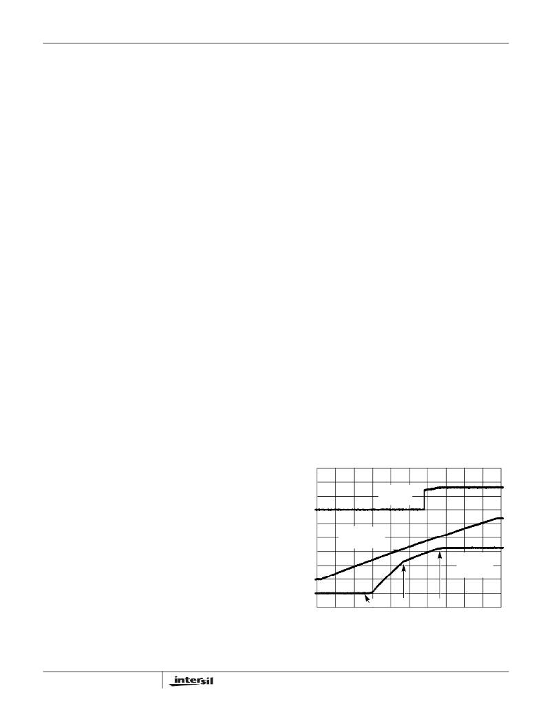
�Soft� Start�
�The� POR� function� initiates� the� soft� start� sequence.� An� internal�
�10μA� current� source� charges� an� external� capacitor� (C� SS� )� on�
�the� SS� pin� to� 4V.� Soft� start� clamps� the� error� amplifier� output�
�(COMP� pin)� and� reference� input� (+� terminal� of� error� amp)� to� the�
�SS� pin� voltage.� Figure� 3� shows� the� soft� start� interval� with�
�C� SS� =� 0.1μF.� Initially� the� clamp� on� the� error� amplifier� (COMP�
�pin)� controls� the� converter’s� output� voltage.� At� t� 1� in� Figure� 3,�
�the� SS� voltage� reaches� the� valley� of� the� oscillator’s� triangle�
�wave.� The� oscillator’s� triangular� waveform� is� compared� to� the�
�ramping� error� amplifier� voltage.� This� generates� PHASE� pulses�
�of� increasing� width� that� charge� the� output� capacitor(s).� This�
�interval� of� increasing� pulse� width� continues� to� t� 2� .� With� sufficient�
�output� voltage,� the� clamp� on� the� reference� input� controls� the�
�output� voltage.� This� is� the� interval� between� t� 2� and� t� 3� in� Figure� 3.�
�At� t� 3� the� SS� voltage� exceeds� the� DACOUT� voltage� and� the�
�output� voltage� is� in� regulation.� This� method� provides� a� rapid�
�and� controlled� output� voltage� rise.� The� PGOOD� signal� toggles�
�‘high’� when� the� output� voltage� (V� SEN� pin)� is� within� ±� 5%� of�
�DACOUT.� The� 2%� hysteresis� built� into� the� power� good�
�comparators� prevents� PGOOD� oscillation� due� to� nominal�
�output� voltage� ripple.�
�PGOOD�
�(2V/DIV)�
�0V�
�SOFT-START�
�(1V/DIV)�
�OUTPUT�
�Fs� ≈� 200kHz� +� ---------------------�
�6�
�5� x� 10�
�R� T� (� k� ?� )�
�(R� T� to� GND)�
�0V�
�VOLTAGE�
�(1V/DIV)�
�0V�
�Conversely,� connecting� a� pull-up� resistor� (R� T� )� from� this� pin�
�t� 1�
�t� 2�
�t� 3�
�to� V� CC� reduces� the� switching� frequency� according� to� the�
�following� equation:�
�TIME� (5ms/DIV)�
�FIGURE� 3.� SOFT� START� INTERVAL�
�Fs� ≈� 200kHz� –� ---------------------�
�7�
�4� x� 10�
�R� T� (� k� ?� )�
�(R� T� to� 12V)�
�6�
�相关PDF资料 |
PDF描述 |
|---|---|
| UVK2V4R7MPD | CAP ALUM 4.7UF 350V 20% RADIAL |
| UVK1V331MPD | CAP ALUM 330UF 35V 20% RADIAL |
| EL7585ILZ | IC POWER SUPPLY TFT-LCD 20-QFN |
| EL7585AILZ-T13 | IC POWER SUPPLY TFT-LCD 20-QFN |
| HSM24DRXH | CONN EDGECARD 48POS DIP .156 SLD |
相关代理商/技术参数 |
参数描述 |
|---|---|
| HIP6004BCBZ | 功能描述:电压模式 PWM 控制器 PWM CNTRLR 3 5 TO 1 3 DAC RNG 20LD RoHS:否 制造商:Texas Instruments 输出端数量:1 拓扑结构:Buck 输出电压:34 V 输出电流: 开关频率: 工作电源电压:4.5 V to 5.5 V 电源电流:600 uA 最大工作温度:+ 125 C 最小工作温度:- 40 C 封装 / 箱体:WSON-8 封装:Reel |
| HIP6004BCBZA | 功能描述:电压模式 PWM 控制器 W/ANNEAL PWM CNTRLR 3 5 TO 1 3 DAC RNG RoHS:否 制造商:Texas Instruments 输出端数量:1 拓扑结构:Buck 输出电压:34 V 输出电流: 开关频率: 工作电源电压:4.5 V to 5.5 V 电源电流:600 uA 最大工作温度:+ 125 C 最小工作温度:- 40 C 封装 / 箱体:WSON-8 封装:Reel |
| HIP6004BCBZA-T | 功能描述:电压模式 PWM 控制器 W/ANNEAL PWM CNTRLR 3 5V TO 1 3V DAC RoHS:否 制造商:Texas Instruments 输出端数量:1 拓扑结构:Buck 输出电压:34 V 输出电流: 开关频率: 工作电源电压:4.5 V to 5.5 V 电源电流:600 uA 最大工作温度:+ 125 C 最小工作温度:- 40 C 封装 / 箱体:WSON-8 封装:Reel |
| HIP6004BCBZ-T | 功能描述:电压模式 PWM 控制器 PWM CNTRLR 3 5V TO 1 3V DAC 20LD TA RoHS:否 制造商:Texas Instruments 输出端数量:1 拓扑结构:Buck 输出电压:34 V 输出电流: 开关频率: 工作电源电压:4.5 V to 5.5 V 电源电流:600 uA 最大工作温度:+ 125 C 最小工作温度:- 40 C 封装 / 箱体:WSON-8 封装:Reel |
| HIP6004BCR | 功能描述:IC CTRLR PWM VOLTAGE MON 20-QFN RoHS:否 类别:集成电路 (IC) >> PMIC - 稳压器 - 专用型 系列:- 产品培训模块:Lead (SnPb) Finish for COTS Obsolescence Mitigation Program 标准包装:2,000 系列:- 应用:电源,ICERA E400,E450 输入电压:4.1 V ~ 5.5 V 输出数:10 输出电压:可编程 工作温度:-40°C ~ 85°C 安装类型:表面贴装 封装/外壳:42-WFBGA,WLCSP 供应商设备封装:42-WLP 包装:带卷 (TR) |
发布紧急采购,3分钟左右您将得到回复。