- 您现在的位置:买卖IC网 > PDF目录371821 > HIP6018 (Intersil Corporation) FPGA - 100000 SYSTEM GATE 2.5 VOLT - NOT RECOMMENDED for NEW DESIGN PDF资料下载
参数资料
| 型号: | HIP6018 |
| 厂商: | Intersil Corporation |
| 元件分类: | FPGA |
| 英文描述: | FPGA - 100000 SYSTEM GATE 2.5 VOLT - NOT RECOMMENDED for NEW DESIGN |
| 中文描述: | 先进的双PWM和线性功率控制 |
| 文件页数: | 12/14页 |
| 文件大小: | 133K |
| 代理商: | HIP6018 |
2-235
microprocessor core requires high quality capacitors to
supply the high slew rate (di/dt) current demands.
PWM Output Capacitors
Modern microprocessors produce transient load rates above
10A/ns. High frequency capacitors initially supply the transient
and slow the current load rate seen by the bulk capacitors.
The bulk filter capacitor values are generally determined by
the ESR (effective series resistance) and ESL (effective series
inductance) parameters rather than actual capacitance.
High frequency decoupling capacitors should be placed as
close to the power pins of the load as physically possible. Be
careful not to add inductance in the circuit board wiring that
could cancel the usefulness of these low inductance
components. Consult with the manufacturer of the load on
specific decoupling requirements.
Use only specialized low-ESR capacitors intended for
switching regulator applications for the bulk capacitors. The
bulk capacitor’s ESR determines the output ripple voltage and
the initial voltage drop after a high slew-rate transient. An
aluminum electrolytic capacitor’s ESR value is related to the
case size with lower ESR available in larger case sizes.
However, the equivalent series inductance of these capacitors
increases with case size and can reduce the usefulness of the
capacitor to high slew-rate transient loading. Unfortunately,
ESL is not a specified parameter. Work with your capacitor
supplier and measure the capacitor’s impedance with
frequency to select suitable components. In most cases,
multiple electrolytic capacitors of small case size perform
better than a single large case capacitor. For a given transient
load magnitude, the output voltage transient response due to
the output capacitor characteristics can be approximated by
the following equation:
Linear Output Capacitors
The output capacitors for the linear regulator and the linear
controller provide dynamic load current. The linear controller
uses dominant pole compensation integrated in the error
amplifier and is insensitive to output capacitor selection.
Capacitor, C
OUT3
should be selected for transient load
regulation.
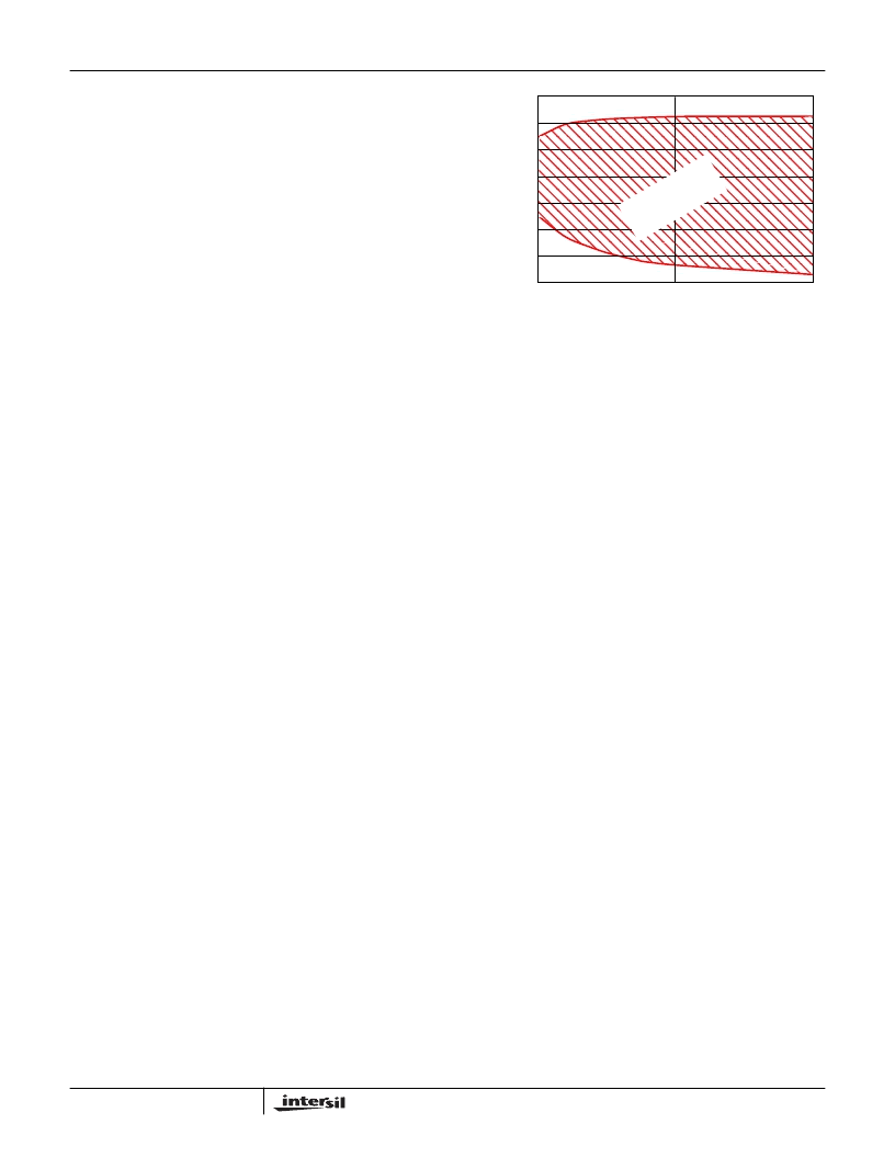
The output capacitor for the linear regulator provides loop
stability. The linear regulator (OUT2) requires an output
capacitor characteristic shown in Figure 13. The upper line
plots the 45 phase margin with 150mA load and the lower
line is the 45 phase margin limit with a 10mA load. Select a
C
OUT2
capacitor with characteristic between the two limits.
Output Inductor Selection
The PWM converter requires an output inductor. The output
inductor is selected to meet the output voltage ripple
requirements and sets the converter’s response time to a
load transient. The inductor value determines the converter’s
ripple current and the ripple voltage is a function of the ripple
current. The ripple voltage and current are approximated by
the following equations:
Increasing the value of inductance reduces the ripple current
and voltage. However, the large inductance values reduce
the converter’s response time to a load transient.
One of the parameters limiting the converter’s response to a
load transient is the time required to change the inductor
current. Given a sufficiently fast control loop design, the
HIP6018 will provide either 0% or 100% duty cycle in
response to a load transient. The response time is the time
interval required to slew the inductor current from an initial
current value to the post-transient current level. During this
interval the difference between the inductor current and the
transient current level must be supplied by the output
capacitors. Minimizing the response time can minimize the
output capacitance required.
The response time to a transient is different for the
application of load and the removal of load. The following
equations give the approximate response time interval for
application and removal of a transient load:
where: I
TRAN
is the transient load current step, t
RISE
is the
response time to the application of load, and t
FALL
is the
response time to the removal of load. With a +5V input
source, the worst case response time can be either at the
application or removal of load, and dependent upon the
output voltage setting. Be sure to check both of these
equations at the minimum and maximum output levels for the
worst case response time.
V
TRAN
ESL
dI
--------------------
×
ESR
I
TRAN
×
+
=
10
1000
100
0.1
0.2
0.3
0.4
0.5
0.6
0.7
CAPACITANCE (
μ
F)
ESR (
)
FIGURE 13. C
OUT2
OUTPUT CAPACITOR
STABLE
I
V
-------------------------------
V
O
–
S
V
IN
---------------
×
=
V
OUT
I
ESR
×
=
t
RISE
L
IN
I
OUT
×
----------–
=
t
FALL
L
------------------------------
I
OUT
×
=
HIP6018
相关PDF资料 |
PDF描述 |
|---|---|
| HIP6018CB | Advanced PWM and Dual Linear Power Control |
| HIP6019BCB | Advanced Dual PWM and Dual Linear Power Control |
| HIP6019B | FPGA - 100000 SYSTEM GATE 2.5 VOLT - NOT RECOMMENDED for NEW DESIGN |
| HIP6028EVAL1 | Advanced PWM and Dual Linear Power Control with Integrated ACPI Support Interface |
| HIP6028 | Advanced PWM and Dual Linear Power Control with Integrated ACPI Support Interface |
相关代理商/技术参数 |
参数描述 |
|---|---|
| HIP6018B | 制造商:INTERSIL 制造商全称:Intersil Corporation 功能描述:Advanced PWM and Dual Linear Power Control |
| HIP6018B_05 | 制造商:INTERSIL 制造商全称:Intersil Corporation 功能描述:Advanced PWM and Dual Linear Power Control |
| HIP6018BCB | 功能描述:IC REG TRPL BCK/LINEAR 24-SOIC RoHS:否 类别:集成电路 (IC) >> PMIC - 稳压器 - 线性 + 切换式 系列:- 标准包装:2,500 系列:- 拓扑:降压(降压)同步(3),线性(LDO)(2) 功能:任何功能 输出数:5 频率 - 开关:300kHz 电压/电流 - 输出 1:控制器 电压/电流 - 输出 2:控制器 电压/电流 - 输出 3:控制器 带 LED 驱动器:无 带监控器:无 带序列发生器:是 电源电压:5.6 V ~ 24 V 工作温度:-40°C ~ 85°C 安装类型:* 封装/外壳:* 供应商设备封装:* 包装:* |
| HIP6018BCB-T | 功能描述:IC REG TRPL BCK/LINEAR 24-SOIC RoHS:否 类别:集成电路 (IC) >> PMIC - 稳压器 - 线性 + 切换式 系列:- 标准包装:2,500 系列:- 拓扑:降压(降压)同步(3),线性(LDO)(2) 功能:任何功能 输出数:5 频率 - 开关:300kHz 电压/电流 - 输出 1:控制器 电压/电流 - 输出 2:控制器 电压/电流 - 输出 3:控制器 带 LED 驱动器:无 带监控器:无 带序列发生器:是 电源电压:5.6 V ~ 24 V 工作温度:-40°C ~ 85°C 安装类型:* 封装/外壳:* 供应商设备封装:* 包装:* |
| HIP6018BCBZ | 功能描述:电压模式 PWM 控制器 ADV DL PWM "3 IN1" W/LWER DAC RNG RoHS:否 制造商:Texas Instruments 输出端数量:1 拓扑结构:Buck 输出电压:34 V 输出电流: 开关频率: 工作电源电压:4.5 V to 5.5 V 电源电流:600 uA 最大工作温度:+ 125 C 最小工作温度:- 40 C 封装 / 箱体:WSON-8 封装:Reel |
发布紧急采购,3分钟左右您将得到回复。