- 您现在的位置:买卖IC网 > PDF目录371821 > HIP6018 (Intersil Corporation) FPGA - 100000 SYSTEM GATE 2.5 VOLT - NOT RECOMMENDED for NEW DESIGN PDF资料下载
参数资料
| 型号: | HIP6018 |
| 厂商: | Intersil Corporation |
| 元件分类: | FPGA |
| 英文描述: | FPGA - 100000 SYSTEM GATE 2.5 VOLT - NOT RECOMMENDED for NEW DESIGN |
| 中文描述: | 先进的双PWM和线性功率控制 |
| 文件页数: | 8/14页 |
| 文件大小: | 133K |
| 代理商: | HIP6018 |
2-231
regulator output or an over-voltage on the PWM output
disables all converters and drives the FAULT pin to VCC.
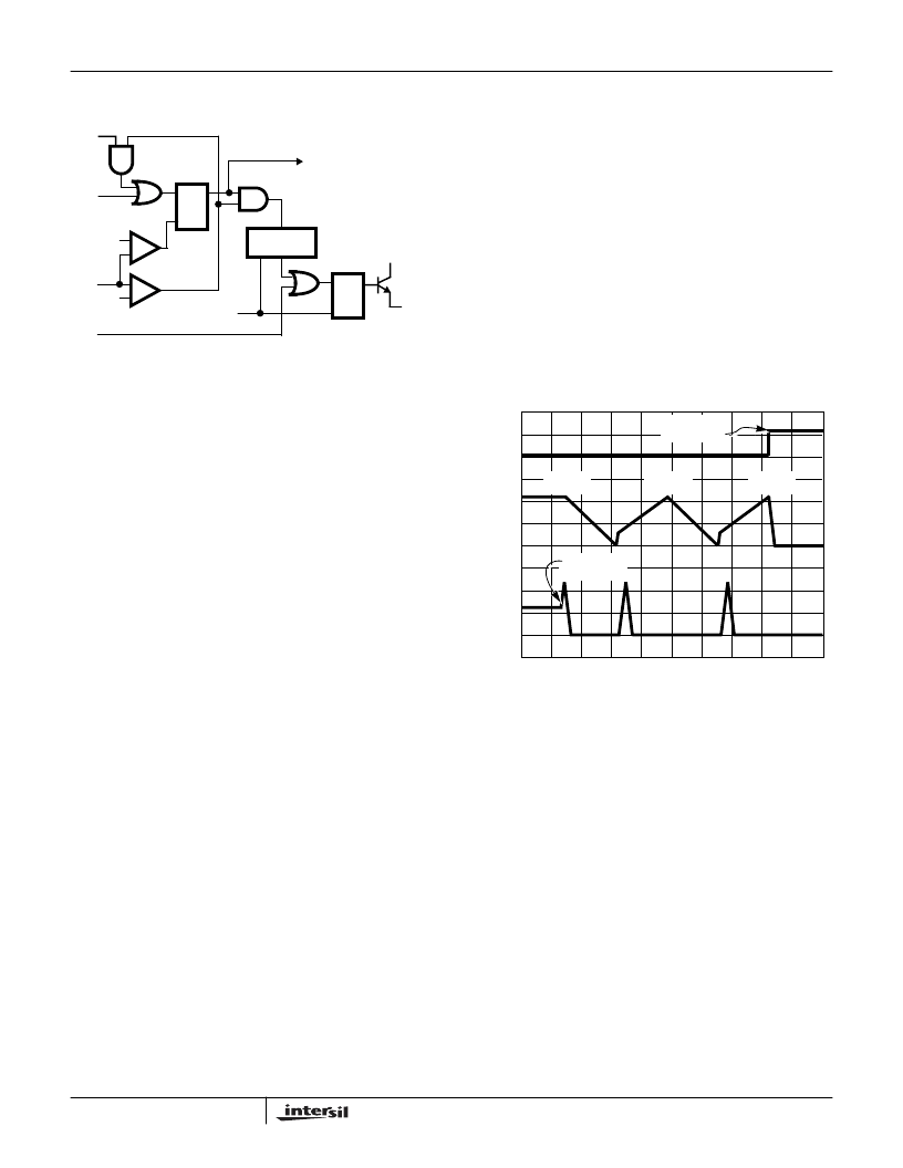
Figure 7 shows a simplified schematic of the fault logic. An
over-voltage detected on VSEN1 immediately sets the fault
latch. A sequence of three over-current fault signals also
sets the fault latch. A comparator indicates when C
SS
is fully
charged (UP signal), such that an under-voltage event on
either linear output (FB2 or FB3) is ignored until after the
soft-start interval (T4 in Figure 6). At startup, this allows
V
OUT2
and V
OUT3
to slew up over increased time intervals,
without generating a fault. Cycling the bias input voltage
(+12V
IN
on the VCC pin) off then on resets the counter and
the fault latch.
Over-Voltage Protection
During operation, a short on the upper PWM MOSFET (Q1)
causes V
OUT1
to increase. When the output exceeds the
over-voltage threshold of 115% (typical) of DACOUT, the
over-voltage comparator trips to set the fault latch and turns
Q2 on as required in order to regulate V
OUT1
to 1.15 x
DACOUT. This blows the input fuse and reduces V
OUT1
.
The fault latch raises the FAULT pin close to VCC potential.
A separate over-voltage circuit provides protection during
the initial application of power. For voltages on the VCC pin
below the power-on reset (and above ~4V), V
OUT1
is
monitored for voltages exceeding 1.26V. Should VSEN1
exceed this level, the lower MOSFET (Q2) is driven on as
needed to regulate V
OUT1
to 1.26V.
Over-Current Protection
All outputs are protected against excessive over-currents.
The PWM controller uses the upper MOSFET’s on-
resistance, r
DS(ON)
to monitor the current for protection
against shorted outputs. The linear regulator monitors the
current of the integrated power device and signals an over-
current condition for currents in excess of 230mA.
Additionally, both the linear regulator and the linear
controller monitor FB2 and FB3 for under-voltage to protect
against excessive currents.
Figures 8 and 9 illustrate the over-current protection with an
overload on OUT1. The overload is applied at T0 and the
current increases through the output inductor (L
OUT1
). At time
T1, the OVER-CURRENT1 comparator trips when the voltage
across Q1 (I
D
r
DS(ON)
) exceeds the level programmed by
R
OCSET
. This inhibits all outputs, discharges the soft-start
capacitor (C
SS
) with a 11
μ
A current sink, and increments the
counter. C
SS
recharges at T2 and initiates a soft-start cycle
with the error amplifiers clamped by soft-start. With OUT1 still
overloaded, the inductor current increases to trip the over-
current comparator. Again, this inhibits all outputs, but the
soft-start voltage continues increasing to 4V before
discharging. The counter increments to 2. The soft-start cycle
repeats at T3 and trips the over-current comparator. The SS
pin voltage increases to 4V at T4 and the counter increments to
3. This sets the fault latch to disable the converter. The fault is
reported on the FAULT pin.
The linear regulator operates in the same way as PWM1 to
over-current faults. Additionally, the linear regulator and
linear controller monitor the feedback pins for an under-
voltage. Should excessive currents cause FB2 or FB3 to fall
below the linear under-voltage threshold, the LUV signal
sets the over-current latch if C
SS
isfully charged. Blanking the
LUV signal during the C
SS
charge interval allows the linear
outputs to build above the under-voltage threshold during
normal start-up. Cycling the bias input power off then on
resets the counter and the fault latch.
Resistor R
OCSET1
programs the over-current trip level for the
PWM converter. As shown in Figure 9, the internal 200
μ
A
current sink develops a voltage across R
OCSET
(V
SET
) that is
referenced to V
IN
. The DRIVE signal enables the over-current
comparator (OVER-CURRENT1). When the voltage across the
upper MOSFET (V
DS(ON)
) exceeds V
SET
, the over-current
comparator trips to set the over-current latch. Both V
SET
and
V
DS
are referenced to V
IN
and a small capacitor across
R
OCSET
helps V
OCSET
track the variations of V
IN
due to
FAULT
LATCH
S
R
Q
POR
COUNTER
OC1
OV
LUV
+
-
+
-
0.15V
4V
SS
VCC
FAULT
R
FIGURE 7. FAULT LOGIC - SIMPLIFIED SCHEMATIC
UP
OVER
CURRENT
LATCH
INHIBIT
S
R
Q
S
0A
0V
2V
4V
FIGURE 8. OVER-CURRENT OPERATION
TIME
T1
T2
T3
T0
T4
F
0V
10V
OVERLOAD
APPLIED
COUNT
= 1
COUNT
= 2
COUNT
= 3
FAULT
REPORTED
HIP6018
相关PDF资料 |
PDF描述 |
|---|---|
| HIP6018CB | Advanced PWM and Dual Linear Power Control |
| HIP6019BCB | Advanced Dual PWM and Dual Linear Power Control |
| HIP6019B | FPGA - 100000 SYSTEM GATE 2.5 VOLT - NOT RECOMMENDED for NEW DESIGN |
| HIP6028EVAL1 | Advanced PWM and Dual Linear Power Control with Integrated ACPI Support Interface |
| HIP6028 | Advanced PWM and Dual Linear Power Control with Integrated ACPI Support Interface |
相关代理商/技术参数 |
参数描述 |
|---|---|
| HIP6018B | 制造商:INTERSIL 制造商全称:Intersil Corporation 功能描述:Advanced PWM and Dual Linear Power Control |
| HIP6018B_05 | 制造商:INTERSIL 制造商全称:Intersil Corporation 功能描述:Advanced PWM and Dual Linear Power Control |
| HIP6018BCB | 功能描述:IC REG TRPL BCK/LINEAR 24-SOIC RoHS:否 类别:集成电路 (IC) >> PMIC - 稳压器 - 线性 + 切换式 系列:- 标准包装:2,500 系列:- 拓扑:降压(降压)同步(3),线性(LDO)(2) 功能:任何功能 输出数:5 频率 - 开关:300kHz 电压/电流 - 输出 1:控制器 电压/电流 - 输出 2:控制器 电压/电流 - 输出 3:控制器 带 LED 驱动器:无 带监控器:无 带序列发生器:是 电源电压:5.6 V ~ 24 V 工作温度:-40°C ~ 85°C 安装类型:* 封装/外壳:* 供应商设备封装:* 包装:* |
| HIP6018BCB-T | 功能描述:IC REG TRPL BCK/LINEAR 24-SOIC RoHS:否 类别:集成电路 (IC) >> PMIC - 稳压器 - 线性 + 切换式 系列:- 标准包装:2,500 系列:- 拓扑:降压(降压)同步(3),线性(LDO)(2) 功能:任何功能 输出数:5 频率 - 开关:300kHz 电压/电流 - 输出 1:控制器 电压/电流 - 输出 2:控制器 电压/电流 - 输出 3:控制器 带 LED 驱动器:无 带监控器:无 带序列发生器:是 电源电压:5.6 V ~ 24 V 工作温度:-40°C ~ 85°C 安装类型:* 封装/外壳:* 供应商设备封装:* 包装:* |
| HIP6018BCBZ | 功能描述:电压模式 PWM 控制器 ADV DL PWM "3 IN1" W/LWER DAC RNG RoHS:否 制造商:Texas Instruments 输出端数量:1 拓扑结构:Buck 输出电压:34 V 输出电流: 开关频率: 工作电源电压:4.5 V to 5.5 V 电源电流:600 uA 最大工作温度:+ 125 C 最小工作温度:- 40 C 封装 / 箱体:WSON-8 封装:Reel |
发布紧急采购,3分钟左右您将得到回复。