- 您现在的位置:买卖IC网 > PDF目录175463 > HUFA75307T3ST (FAIRCHILD SEMICONDUCTOR CORP) 2.6A, 55V, 0.090 Ohm, N-Channel UltraFET Power MOSFET PDF资料下载
参数资料
| 型号: | HUFA75307T3ST |
| 厂商: | FAIRCHILD SEMICONDUCTOR CORP |
| 元件分类: | JFETs |
| 英文描述: | 2.6A, 55V, 0.090 Ohm, N-Channel UltraFET Power MOSFET |
| 中文描述: | 2.6 A, 55 V, 0.09 ohm, N-CHANNEL, Si, POWER, MOSFET |
| 文件页数: | 2/9页 |
| 文件大小: | 174K |
| 代理商: | HUFA75307T3ST |
2001 Fairchild Semiconductor Corporation
HUFA75307T3ST Rev. B
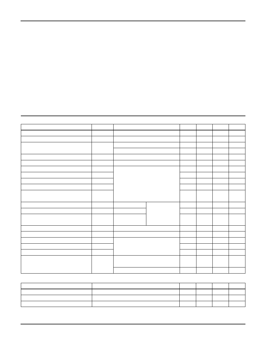
Absolute Maximum Ratings
TA = 25
oC, Unless Otherwise Specified
UNITS
Drain to Source Voltage (Note 1). . . . . . . . . . . . . . . . . . . . . . . . . . . . . . . . . . . . . . . . . . . . VDSS
55
V
Drain to Gate Voltage (RGS = 20k) (Note 1) . . . . . . . . . . . . . . . . . . . . . . . . . . . . . . . . . VDGR
55
V
Gate to Source Voltage . . . . . . . . . . . . . . . . . . . . . . . . . . . . . . . . . . . . . . . . . . . . . . . . . . . VGS
±20V
V
Drain Current
Continuous (Figure 2) (Note 2). . . . . . . . . . . . . . . . . . . . . . . . . . . . . . . . . . . . . . . . . . . . . . ID
Pulsed Drain Current . . . . . . . . . . . . . . . . . . . . . . . . . . . . . . . . . . . . . . . . . . . . . . . . . . . . IDM
2.6
Figure 5
A
Pulsed Avalanche Rating. . . . . . . . . . . . . . . . . . . . . . . . . . . . . . . . . . . . . . . . . . . . . . . . . . . EAS
Figures 6, 14, 15
Power Dissipation (Note 2) . . . . . . . . . . . . . . . . . . . . . . . . . . . . . . . . . . . . . . . . . . . . . . . . . . PD
Derate Above 25oC . . . . . . . . . . . . . . . . . . . . . . . . . . . . . . . . . . . . . . . . . . . . . . . . . . . . . . . .
1.1
9.09
W
mW/oC
Operating and Storage Temperature . . . . . . . . . . . . . . . . . . . . . . . . . . . . . . . . . . . . . . TJ, TSTG
-55 to 150
oC
Maximum Temperature for Soldering
Leads at 0.063in (1.6mm) from Case for 10s. . . . . . . . . . . . . . . . . . . . . . . . . . . . . . . . . . . TL
Package Body for 10s, See Techbrief 334. . . . . . . . . . . . . . . . . . . . . . . . . . . . . . . . . . . Tpkg
300
260
oC
CAUTION: Stresses above those listed in “Absolute Maximum Ratings” may cause permanent damage to the device. This is a stress only rating and operation of the
device at these or any other conditions above those indicated in the operational sections of this specification is not implied.
NOTE:
1. TJ = 25
oC to 125oC.
Electrical Specifications
TA = 25
oC, Unless Otherwise Specified
PARAMETER
SYMBOL
TEST CONDITIONS
MIN
TYP
MAX
UNITS
Drain to Source Breakdown Voltage
BVDSS
ID = 250A, VGS = 0V (Figure 11)
55
-
V
Gate to Source Threshold Voltage
VGS(TH)
VGS = VDS, ID = 250A (Figure 10)
2
-
4
V
Zero Gate Voltage Drain Current
IDSS
VDS = 50V, VGS = 0V
-
1
A
VDS = 45V, VGS = 0V, TA = 150
oC
-
250
A
Gate to Source Leakage Current
IGSS
VGS = ±20V
-
100
nA
Drain to Source On Resistance
rDS(ON)
ID = 2.6A, VGS = 10V) (Figure 9)
-
0.070
0.090
Turn-On Time
tON
VDD = 30V, ID 2.6A,
RL = 11.5, VGS = 10V,
RGS = 25
-
55
ns
Turn-On Delay Time
td(ON)
-5
-
ns
Rise Time
tr
-30-
ns
Turn-Off Delay Time
td(OFF)
-35-
ns
Fall Time
tf
-25-
ns
Turn-Off Time
tOFF
-
90
ns
Total Gate Charge
Qg(TOT)
VGS = 0V to 20V
VDD = 30V,
ID 2.6A,
RL = 11.5
Ig(REF) = 1.0mA
(Figure 13)
-14
17
nC
Gate Charge at 10V
Qg(10)
VGS = 0V to 10V
-
8.3
10
nC
Threshold Gate Charge
Qg(TH)
VGS = 0V to 2V
-
0.6
0.8
nC
Gate to Source Gate Charge
Qgs
-
1.00
-
nC
Gate to Drain “Miller” Charge
Qgd
-
4.00
-
nC
Input Capacitance
CISS
VDS = 25V, VGS = 0V,
f = 1MHz
(Figure 12)
-
250
-
pF
Output Capacitance
COSS
-
115
-
pF
Reverse Transfer Capacitance
CRSS
-30-
pF
Thermal Resistance Junction to Ambient
RθJA
Pad Area = 0.171 in2 (see note 2)
-
110
oC/W
Pad Area = 0.068 in2
-
128
oC/W
Pad Area = 0.026 in2
-
147
oC/W
Source to Drain Diode Specifications
PARAMETER
SYMBOL
TEST CONDITIONS
MIN
TYP
MAX
UNITS
Source to Drain Diode Voltage
VSD
ISD = 2.6A
-
1.25
V
Reverse Recovery Time
trr
ISD = 2.6A, dISD/dt = 100A/s-
-
40
ns
Reverse Recovered Charge
QRR
ISD = 2.6A, dISD/dt = 100A/s-
-
50
nC
NOTE:
2. 110 oC/W measured using FR-4 board with 0.171in2 footprint for 1000s.
HUFA75307T3ST
相关PDF资料 |
PDF描述 |
|---|---|
| HUFA75309D3 | 19A, 55V, 0.070 Ohm, N-Channel UltraFET Power MOSFETs |
| HUFA75309D3S | 19A, 55V, 0.070 Ohm, N-Channel UltraFET Power MOSFETs |
| HUFA75309P3 | 19A, 55V, 0.070 Ohm, N-Channel UltraFET Power MOSFETs |
| HUFA75309T3ST | 3A, 55V, 0.070 Ohm, N-Channel UltraFET Power MOSFET |
| HUFA75321D3 | 20A, 55V, 0.036 Ohm, N-Channel UltraFET Power MOSFETs |
相关代理商/技术参数 |
参数描述 |
|---|---|
| HUFA75309D3 | 功能描述:MOSFET 19a 55V N-Channel UltraFET RoHS:否 制造商:STMicroelectronics 晶体管极性:N-Channel 汲极/源极击穿电压:650 V 闸/源击穿电压:25 V 漏极连续电流:130 A 电阻汲极/源极 RDS(导通):0.014 Ohms 配置:Single 最大工作温度: 安装风格:Through Hole 封装 / 箱体:Max247 封装:Tube |
| HUFA75309D3S | 功能描述:MOSFET 19a 55V N-Channel UltraFET RoHS:否 制造商:STMicroelectronics 晶体管极性:N-Channel 汲极/源极击穿电压:650 V 闸/源击穿电压:25 V 漏极连续电流:130 A 电阻汲极/源极 RDS(导通):0.014 Ohms 配置:Single 最大工作温度: 安装风格:Through Hole 封装 / 箱体:Max247 封装:Tube |
| HUFA75309D3ST | 功能描述:MOSFET 19a 55V N-Channel UltraFET RoHS:否 制造商:STMicroelectronics 晶体管极性:N-Channel 汲极/源极击穿电压:650 V 闸/源击穿电压:25 V 漏极连续电流:130 A 电阻汲极/源极 RDS(导通):0.014 Ohms 配置:Single 最大工作温度: 安装风格:Through Hole 封装 / 箱体:Max247 封装:Tube |
| HUFA75309P3 | 功能描述:MOSFET 19a 55V N-Channel UltraFET RoHS:否 制造商:STMicroelectronics 晶体管极性:N-Channel 汲极/源极击穿电压:650 V 闸/源击穿电压:25 V 漏极连续电流:130 A 电阻汲极/源极 RDS(导通):0.014 Ohms 配置:Single 最大工作温度: 安装风格:Through Hole 封装 / 箱体:Max247 封装:Tube |
| HUFA75309T3ST | 功能描述:MOSFET 19a 55V N-Channel UltraFET RoHS:否 制造商:STMicroelectronics 晶体管极性:N-Channel 汲极/源极击穿电压:650 V 闸/源击穿电压:25 V 漏极连续电流:130 A 电阻汲极/源极 RDS(导通):0.014 Ohms 配置:Single 最大工作温度: 安装风格:Through Hole 封装 / 箱体:Max247 封装:Tube |
发布紧急采购,3分钟左右您将得到回复。