- 您现在的位置:买卖IC网 > PDF目录384468 > HY5PS1G831CLFP-C4 (HYNIX SEMICONDUCTOR INC) 1Gb DDR2 SDRAM PDF资料下载
参数资料
| 型号: | HY5PS1G831CLFP-C4 |
| 厂商: | HYNIX SEMICONDUCTOR INC |
| 元件分类: | DRAM |
| 英文描述: | 1Gb DDR2 SDRAM |
| 中文描述: | 128M X 8 DDR DRAM, 0.5 ns, PBGA60 |
| 封装: | ROHS COMPLIANT, FBGA-60 |
| 文件页数: | 17/37页 |
| 文件大小: | 539K |
| 代理商: | HY5PS1G831CLFP-C4 |
第1页第2页第3页第4页第5页第6页第7页第8页第9页第10页第11页第12页第13页第14页第15页第16页当前第17页第18页第19页第20页第21页第22页第23页第24页第25页第26页第27页第28页第29页第30页第31页第32页第33页第34页第35页第36页第37页
Rev. 0.2 / Dec 2006
17
HY5PS1G431C(L)FP
HY5PS1G831C(L)FP
HY5PS1G1631C(L)FP
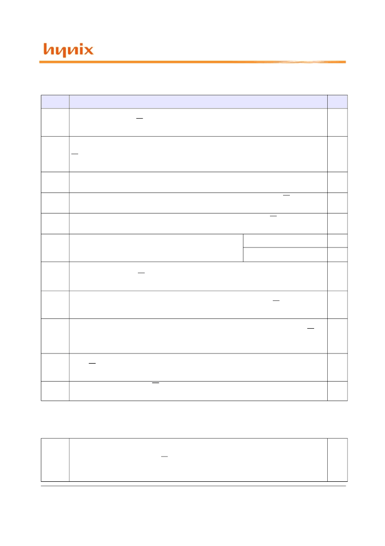
IDD Test Conditions
(IDD values are for full operating range of Voltage and Temperature, Notes 1-5)
Symbol
Conditions
Units
IDD0
Operating one bank active-precharge current
; tCK = tCK(IDD), tRC = tRC(IDD), tRAS = tRAS
min(IDD) ; CKE is HIGH, CS is HIGH between valid commands;Address bus inputs are SWITCH-
ING;Data bus inputs are SWITCHING
mA
IDD1
Operating one bank active-read-precharge
χυρρεντ
; IOUT = 0mA;BL = 4, CL = CL(IDD), AL
= 0; tCK = tCK(IDD), tRC = tRC (IDD), tRAS = tRASmin(IDD), tRCD = tRCD(IDD) ; CKE is HIGH,
CS is HIGH between valid commands ; Address bus inputs are SWITCHING ; Data pattern is same
as IDD4W
mA
IDD2P
Precharge power-down current
; All banks idle ; tCK = tCK(IDD) ; CKE is LOW ; Other control
and address bus inputs are STABLE; Data bus inputs are FLOATING
mA
IDD2Q
Precharge quiet standby current
;All banks idle; tCK = tCK(IDD);CKE is HIGH, CS is HIGH;
Other control and address bus inputs are STABLE; Data bus inputs are FLOATING
mA
IDD2N
Precharge standby current
; All banks idle; tCK = tCK(IDD); CKE is HIGH, CS is HIGH; Other
control and address bus inputs are SWITCHING; Data bus inputs are SWITCHING
mA
IDD3P
Active power-down current
; All banks open; tCK = tCK(IDD);
CKE is LOW; Other control and address bus inputs are STABLE;
Data bus inputs are FLOATING
Fast PDN Exit MRS(12) = 0
mA
Slow PDN Exit MRS(12) = 1
mA
IDD3N
Active standby current
; All banks open; tCK = tCK(IDD), tRAS = tRASmax(IDD), tRP
=tRP(IDD); CKE is HIGH, CS is HIGH between valid commands; Other control and address bus
inputs are SWITCHING; Data bus inputs are SWITCHING
mA
IDD4W
Operating burst write current
; All banks open, Continuous burst writes; BL = 4, CL = CL(IDD),
AL = 0; tCK = tCK(IDD), tRAS = tRASmax(IDD), tRP = tRP(IDD); CKE is HIGH, CS is HIGH between
valid commands; Address bus inputs are SWITCHING; Data bus inputs are SWITCHING
mA
IDD4R
Operating burst read current
; All banks open, Continuous burst reads, IOUT = 0mA; BL = 4, CL
= CL(IDD), AL = 0; tCK = tCK(IDD), tRAS = tRASmax(IDD), tRP = tRP(IDD); CKE is HIGH, CS is
HIGH between valid commands; Address bus inputs are SWITCHING;; Data pattern is same as
IDD4W
mA
IDD5B
Burst refresh current
; tCK = tCK(IDD); Refresh command at every tRFC(IDD) interval; CKE is
HIGH, CS is HIGH between valid commands; Other control and address bus inputs are SWITCH-
ING; Data bus inputs are SWITCHING
mA
IDD6
Self refresh current
; CK and CK at 0V; CKE £ 0.2V; Other control and address bus inputs are
FLOATING; Data bus inputs are FLOATING
mA
FLOATING is defined as inputs at VREF = VDDQ/2
SWITCHING is defined as: inputs changing between HIGH and LOW every other clock cycle (once per two clocks)
for address and control signals, and inputs changing between HIGH and LOW every other data transfer (once per
clock) for DQ signals not including masks or strobes.
IDD7
Operating bank interleave read current
; All bank interleaving reads, IOUT = 0mA; BL = 4, CL
= CL(IDD), AL = tRCD(IDD)-1*tCK(IDD); tCK = tCK(IDD), tRC = tRC(IDD), tRRD = tRRD(IDD),
tRCD = 1*tCK(IDD); CKE is HIGH, CS is HIGH between valid commands; Address bus inputs are
STABLE during DESELECTs; Data pattern is same as IDD4R; - Refer to the following page for
detailed timing conditions
mA
相关PDF资料 |
PDF描述 |
|---|---|
| HY5PS1G831CLFP-E3 | 1Gb DDR2 SDRAM |
| HY5PS1G831CLFP-S5 | 1Gb DDR2 SDRAM |
| HY5PS1G831CLFP-Y5 | 1Gb DDR2 SDRAM |
| HY5PS1G821LM-E3 | 1Gb DDR2 SDRAM(DDP) |
| HY5PS1G821M | 1Gb DDR2 SDRAM(DDP) |
相关代理商/技术参数 |
参数描述 |
|---|---|
| HY5PS1G831CLFP-E3 | 制造商:HYNIX 制造商全称:Hynix Semiconductor 功能描述:1Gb DDR2 SDRAM |
| HY5PS1G831CLFP-S5 | 制造商:HYNIX 制造商全称:Hynix Semiconductor 功能描述:1Gb DDR2 SDRAM |
| HY5PS1G831CLFP-Y5 | 制造商:HYNIX 制造商全称:Hynix Semiconductor 功能描述:1Gb DDR2 SDRAM |
| HY5PS1G831F | 制造商:HYNIX 制造商全称:Hynix Semiconductor 功能描述:1Gb DDR2 SDRAM |
| HY5PS1G831F-C4 | 制造商:HYNIX 制造商全称:Hynix Semiconductor 功能描述:1Gb DDR2 SDRAM |
发布紧急采购,3分钟左右您将得到回复。