- 您现在的位置:买卖IC网 > PDF目录223993 > HY5V28CLF-S (HYNIX SEMICONDUCTOR INC) 16M X 8 SYNCHRONOUS DRAM, 6 ns, PBGA54 PDF资料下载
参数资料
| 型号: | HY5V28CLF-S |
| 厂商: | HYNIX SEMICONDUCTOR INC |
| 元件分类: | DRAM |
| 英文描述: | 16M X 8 SYNCHRONOUS DRAM, 6 ns, PBGA54 |
| 封装: | 8.30 X 10.50 MM, 0.80 MM PITCH, FBGA-54 |
| 文件页数: | 1/14页 |
| 文件大小: | 128K |
| 代理商: | HY5V28CLF-S |
HY5V28C(L)F
4Banks x 4M x 8bits Synchronous DRAM
This document is a general product description and is subject to change without notice. Hynix does not assume any responsibility for
use of circuits described. No patent licenses are implied.
Rev. 0.1/Sep. 01
DESCRIPTION
The Hynix HY5V28C(L)F is a 134,217,728bit CMOS Synchronous DRAM, ideally suited for the main memory applica-
tions which require large memory density and high bandwidth. HY5V28C(L)F is organized as 4banks of 4,194,304x8.
HY5V28C(L)F is offering fully synchronous operation referenced to a positive edge of the clock. All inputs and outputs
are synchronized with the rising edge of the clock input. The data paths are internally pipelined to achieve very high
bandwidth. All input and output voltage levels are compatible with LVTTL.
Programmable options include the length of pipeline (Read latency of 2 or 3), the number of consecutive read or write
cycles initiated by a single control command (Burst length of 1,2,4,8 or full page), and the burst count
sequence(sequential or interleave). A burst of read or write cycles in progress can be terminated by a burst terminate
command or can be interrupted and replaced by a new burst read or write command on any cycle. (This pipelined
design is not restricted by a `2N` rule.)
FEATURES
Single 3.3
±0.3V power supply
All device Balls are compatible with LVTTL interface
54Ball FBGA With 0.8mm of ball pitch
All inputs and outputs referenced to positive edge of
system clock
Data mask function by DQM
Internal four banks operation
Auto refresh and self refresh
4096 refresh cycles / 64ms
Programmable Burst Length and Burst Type
- 1, 2, 4, 8 or Full Page for Sequential Burst
- 1, 2, 4 or 8 for Interleave Burst
Programmable CAS Latency ; 2, 3 Clocks
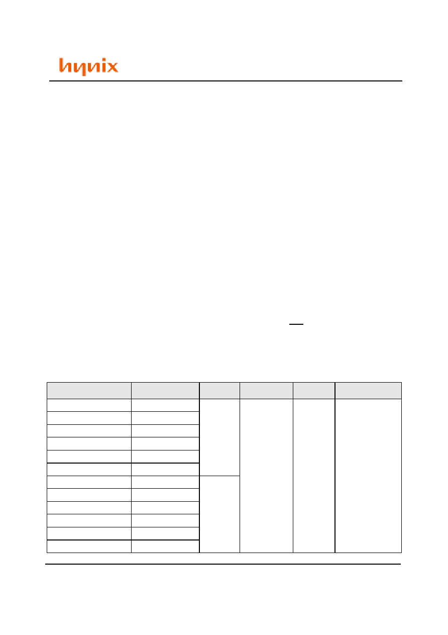
ORDERING INFORMATION
Part No.
Clock Frequency
Power
Organization
Interface
Package
HY5V28CF-6
166MHz
Normal
4Banks x 4Mbits
x 8
LVTTL
54Ball FBGA
HY5V28CF-K
133MHz
HY5V28CF-H
133MHz
HY5V28CF-8
125MHz
HY5V28CF-P
100MHz
HY5V28CF-S
100MHz
HY5V28CLF-6
166MHz
Low power
HY5V28CLF-K
133MHz
HY5V28CLF-H
133MHz
HY5V28CLF-8
125MHz
HY5V28CLF-P
100MHz
HY5V28CLF-S
100MHz
相关PDF资料 |
PDF描述 |
|---|---|
| HY5V52CLF-6 | 8M X 32 SYNCHRONOUS DRAM, 5.4 ns, PBGA90 |
| HY5V52EMP-H | 8M X 32 SYNCHRONOUS DRAM, 5.4 ns, PBGA90 |
| HY5V56BSF-8 | 16M X 16 SYNCHRONOUS DRAM, 6 ns, PBGA54 |
| HY62256ALLR1-70 | x8 SRAM |
| HY62256ALLR1-85 | x8 SRAM |
相关代理商/技术参数 |
参数描述 |
|---|---|
| HY5V52CF | 制造商:未知厂家 制造商全称:未知厂家 功能描述:8Mx32|3.3V|8K|H/8/P/S|SDR SDRAM - 256M |
| HY5V52CFP6 | 制造商:HYNIX 功能描述:Pb Free |
| HY5V52F | 制造商:HYNIX 制造商全称:Hynix Semiconductor 功能描述:4Banks x 2M x 32bits Synchronous DRAM |
| HY5V52F-H | 制造商:HYNIX 制造商全称:Hynix Semiconductor 功能描述:4Banks x 2M x 32bits Synchronous DRAM |
| HY5V52F-P | 制造商:HYNIX 制造商全称:Hynix Semiconductor 功能描述:4Banks x 2M x 32bits Synchronous DRAM |
发布紧急采购,3分钟左右您将得到回复。