- 您现在的位置:买卖IC网 > PDF目录223993 > HY5V28CLF-S (HYNIX SEMICONDUCTOR INC) 16M X 8 SYNCHRONOUS DRAM, 6 ns, PBGA54 PDF资料下载
参数资料
| 型号: | HY5V28CLF-S |
| 厂商: | HYNIX SEMICONDUCTOR INC |
| 元件分类: | DRAM |
| 英文描述: | 16M X 8 SYNCHRONOUS DRAM, 6 ns, PBGA54 |
| 封装: | 8.30 X 10.50 MM, 0.80 MM PITCH, FBGA-54 |
| 文件页数: | 8/14页 |
| 文件大小: | 128K |
| 代理商: | HY5V28CLF-S |
HY5V28C(L)F
Rev. 0.1/Sep. 01
4
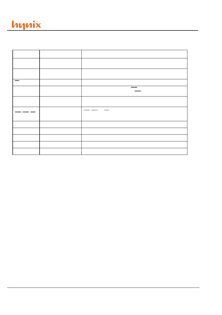
Ball DESCRIPTION
Ball
Ball NAME
DESCRIPTION
CLK
Clock
The system clock input. All other inputs are registered to the SDRAM on the
rising edge of CLK
CKE
Clock Enable
Controls internal clock signal and when deactivated, the SDRAM will be one
of the states among power down, suspend or self refresh
CS
Chip Select
Enables or disables all inputs except CLK, CKE and DQM
BA0, BA1
Bank Address
Selects bank to be activated during RAS activity
Selects bank to be read/written during CAS activity
A0 ~ A11
Address
Row Address : RA0 ~ RA11, Column Address : CA0 ~ CA9
Auto-precharge flag : A10
RAS, CAS, WE
Row Address Strobe, Col-
umn Address Strobe, Write
Enable
RAS, CAS and WE define the operation
Refer function truth table for details
DQM
Data Input/Output Mask
Controls output buffers in read mode and masks input data in write mode
DQ0 ~ DQ7
Data Input/Output
Multiplexed data input / output Ball
VDD/VSS
Power Supply/Ground
Power supply for internal circuits and input buffers
VDDQ/VSSQ
Data Output Power/Ground
Power supply for output buffers
NC
No Connection
No connection
相关PDF资料 |
PDF描述 |
|---|---|
| HY5V52CLF-6 | 8M X 32 SYNCHRONOUS DRAM, 5.4 ns, PBGA90 |
| HY5V52EMP-H | 8M X 32 SYNCHRONOUS DRAM, 5.4 ns, PBGA90 |
| HY5V56BSF-8 | 16M X 16 SYNCHRONOUS DRAM, 6 ns, PBGA54 |
| HY62256ALLR1-70 | x8 SRAM |
| HY62256ALLR1-85 | x8 SRAM |
相关代理商/技术参数 |
参数描述 |
|---|---|
| HY5V52CF | 制造商:未知厂家 制造商全称:未知厂家 功能描述:8Mx32|3.3V|8K|H/8/P/S|SDR SDRAM - 256M |
| HY5V52CFP6 | 制造商:HYNIX 功能描述:Pb Free |
| HY5V52F | 制造商:HYNIX 制造商全称:Hynix Semiconductor 功能描述:4Banks x 2M x 32bits Synchronous DRAM |
| HY5V52F-H | 制造商:HYNIX 制造商全称:Hynix Semiconductor 功能描述:4Banks x 2M x 32bits Synchronous DRAM |
| HY5V52F-P | 制造商:HYNIX 制造商全称:Hynix Semiconductor 功能描述:4Banks x 2M x 32bits Synchronous DRAM |
发布紧急采购,3分钟左右您将得到回复。