- 您现在的位置:买卖IC网 > PDF目录296204 > ICD2053BSC-1 (CYPRESS SEMICONDUCTOR CORP) 100 MHz, OTHER CLOCK GENERATOR, PDSO8 PDF资料下载
参数资料
| 型号: | ICD2053BSC-1 |
| 厂商: | CYPRESS SEMICONDUCTOR CORP |
| 元件分类: | XO, clock |
| 英文描述: | 100 MHz, OTHER CLOCK GENERATOR, PDSO8 |
| 封装: | 0.150 INCH, SOIC-8 |
| 文件页数: | 3/9页 |
| 文件大小: | 138K |
| 代理商: | ICD2053BSC-1 |
ICD2053B
Document #: 38-07134 Rev. **
Page 3 of 9
Program Register
The Program register can be loaded with a 22-bit program-
ming word, the fields of which are defined in Table 2.
The VCO frequency, f(VCO), is determined by the following re-
lation:
f(VCO) = (2 * f(REF) *
P/
Q)
where
P’ = P
3
Q’ = Q
2
f(REF) = Reference frequency (1 MHz to 25 MHz)
The value of f(VCO) must remain between 50 MHz and 150 MHz.
Therefore, for output frequencies below 50 MHz, f(VCO) must be
brought into range. To accomplish this, a post-VCO Divisor is select-
ed by setting the values of the Max field (M) as follows:
The index field (I) is used to preset the VCO to an appropriate
range. The value for this field should be chosen from the fol-
lowing table. (Note that this table is referenced to the VCO
frequency f(VCO) rather than to thedesired output frequencyand that
only the MSB is significant.)
To assist with these calculations, Cypress/IC Designs provides
the BITCALC program. BITCALC is a Windows program for
the IBM PC which automatically generates the appropriate program-
ming word from the user’s reference input and desired output fre-
quencies.
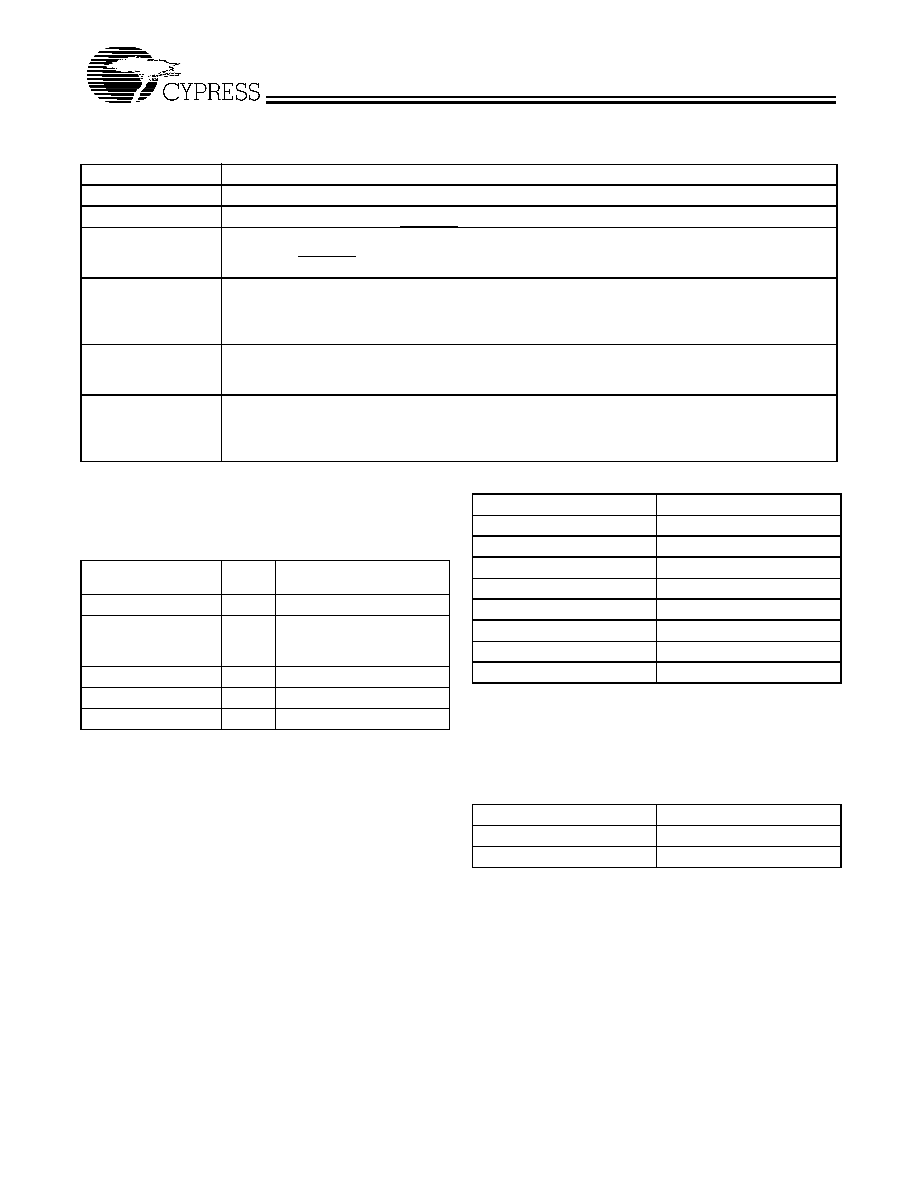
Table 1. Control Register
Bit
Definition
RESERVED
For future use. Set to 0.
Duty Cycle Adjust
Set to 1 to reduce duty cycle by approximately 0.7 ns. Normally set to 1.
Pin 7 Usage
Definition of whether pin 7 is MUXREF or OE input pin
0 = Pin 7 is OE input
(default)
1 = Pin 7 is MUXREF input
MUXREF Control
Allows internal control of MUXREF. If enabled, this feature automatically multiplexes the reference
frequency to the CLKOUT output. This is used to change output glitch-free to new frequencies.
0 = CLKOUT is VCO frequency
1 = CLKOUT is f(REF)
(default)
OE Control
Forces the CLKOUT output into a three-state mode
0 = CLKOUT is VCO frequency or f(REF)
(default) (depending on current MUXREF state)
1 = CLKOUT is three-stated
Enable Program
Word
Enable Program word loading into Program register. When enabled, the Program word may be shifted
in. This permits changing the Control register without disturbing Program register data.
0 = Program register is disabled from loading
(default)
1 = Program register is enabled to receive data
Table 2. Program Register
Field
# of
Bits
Notes
P Counter value (P’)
7
MSB (Most Significant Bits)
Duty Cycle Adjust Up
(D)
1
Set to logic 1 to increase
duty cycle by Pyrex. 0.7 ns.
Normally set to 1.
Max (M)
3
Q Counter value (Q’)
7
Index (I)
4
LSB (Least Significant Bits)
Mux Field (M)
M
Divisor
000
1
001
2
010
4
011
8
100
16
101
32
110
64
111
128
Index Field (I)
I
f(VCO) @ 5V
0000
50 to 80 MHz
1000
80 to 150 MHz
相关PDF资料 |
PDF描述 |
|---|---|
| ICE-063-SD2-TG30 | DIP6, IC SOCKET |
| ICE-223-SD2-TG30 | DIP22, IC SOCKET |
| ICE-223-SD2-TT | DIP22, IC SOCKET |
| ICE-224-SD2-TG | DIP22, IC SOCKET |
| ICE-244-SD2-TG | DIP24, IC SOCKET |
相关代理商/技术参数 |
参数描述 |
|---|---|
| ICD2061A | 制造商:未知厂家 制造商全称:未知厂家 功能描述:Video/Graphics Clock Generator |
| ICD2061ASC | 制造商:未知厂家 制造商全称:未知厂家 功能描述:Video/Graphics Clock Generator |
| ICD2061ASC1 | 制造商:ICD 功能描述:2061 CDESIGN S8G1B |
| ICD2061ASC-1 | 制造商:ICD 功能描述:2061 CDESIGN S8G1B |
| ICD2061CC-1 | 制造商:未知厂家 制造商全称:未知厂家 功能描述:Video/Graphics Clock Generator |
发布紧急采购,3分钟左右您将得到回复。