- 您现在的位置:买卖IC网 > PDF目录296204 > ICD2053BSC-1 (CYPRESS SEMICONDUCTOR CORP) 100 MHz, OTHER CLOCK GENERATOR, PDSO8 PDF资料下载
参数资料
| 型号: | ICD2053BSC-1 |
| 厂商: | CYPRESS SEMICONDUCTOR CORP |
| 元件分类: | XO, clock |
| 英文描述: | 100 MHz, OTHER CLOCK GENERATOR, PDSO8 |
| 封装: | 0.150 INCH, SOIC-8 |
| 文件页数: | 6/9页 |
| 文件大小: | 138K |
| 代理商: | ICD2053BSC-1 |
ICD2053B
Document #: 38-07134 Rev. **
Page 6 of 9
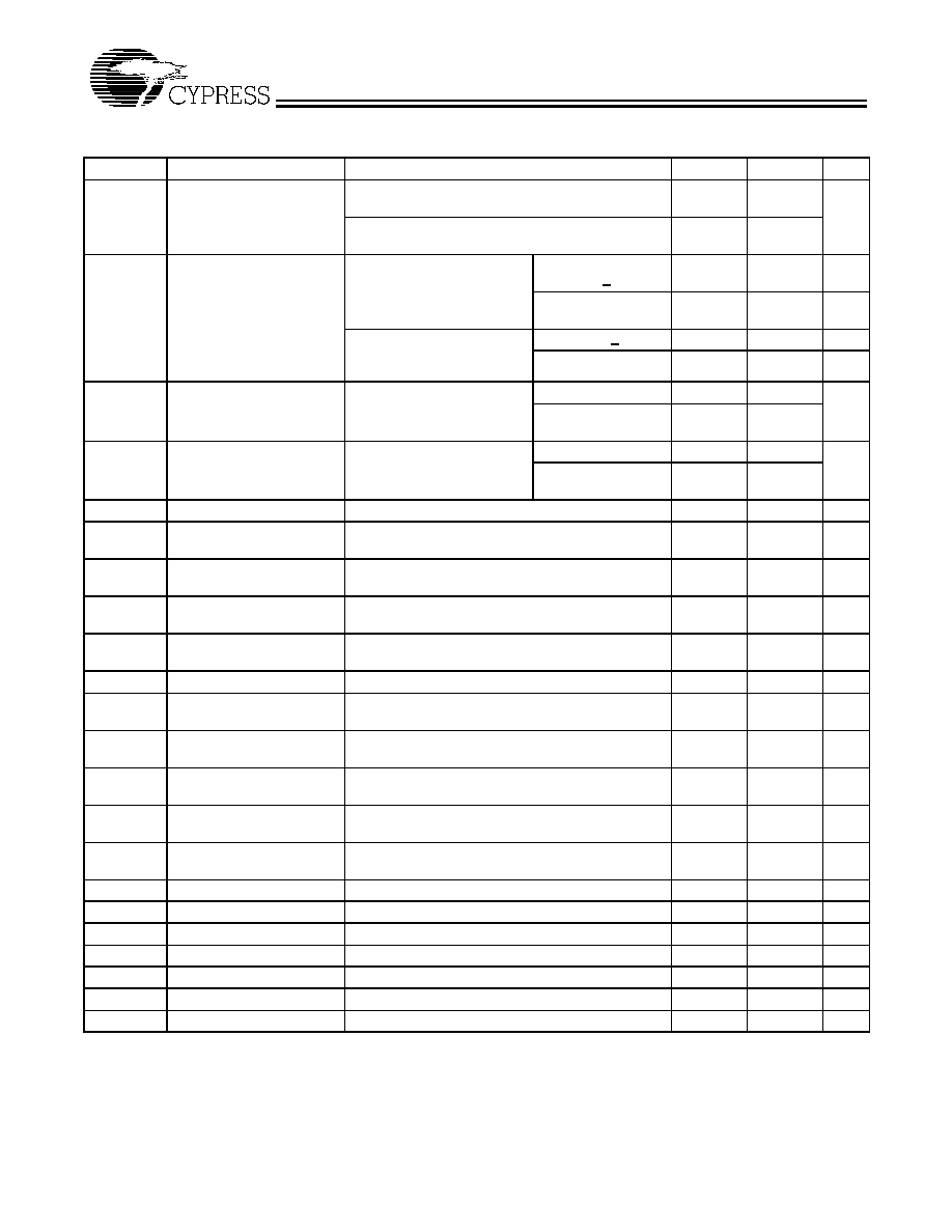
t2
Output Period
CLKOUT period (frequency), TTL levels
10 (100
MHz)
2560
(391 kHz)
ns
CLKOUT period (frequency), CMOS levels
11.1 (90
MHz)
2560
(391 kHz)
t3
Output Duty Cycle (t0/t2)
Duty cycle of CLKOUT
measured at 1.4V (TTL)
threshold
f(OUT) < 50 MHz AND
post-divide > 2
45%
55%
f(OUT) > 50 MHz OR
post-divide = 1
40%
60%
Duty cycle of CLKOUT
measured at VDD/2 (CMOS)
threshold
post-divide > 2
45%
55%
post-divide = 1
40%
60%
t4
Rise Time
Rise time for the clock output
into a 25 pF load
TTL 0.4V to 2.4V
3
ns
CMOS, 0.1VDD to
0.9VDD
6
t5
Fall Time
Fall time for the clock output
into a 25 pF load
TTL 0.4V to 2.4V
3
ns
CMOS, 0.1VDD to
0.9VDD
6
t6
SCLK HIGH Time
Minimum HIGH time for the SCLK clock
450
ns
t7
Clock Valid
Time required for the CLKOUT oscillator to become
valid after last SCLK clock[5]
t(REF)
3 * t(REF)
+ 25
ns
t8
Serial Data Set-up
Time required for the data to be valid prior to the
rising edge of SCLK
15
ns
t9
Hold
Time required for the data to remain valid after the
rising edge of SCLK
0
ns
t10
Delay, MUXREF[6] Asserted
to CLKOUT HIGH
Time for CLKOUT to go HIGH after assertion of
MUXREF[6]
0
told + 25
ns
t11
Transition, f(OLD) to f(REF)
Delay of first falling edge of f(REF) signal at output
t13
t(REF) + 25
ns
t12
Reference Output High
Time
Output during MUXREF[6], reference DC coupled
t16 10
t16 + 10
ns
t13
Reference Output Low
Time
Output during MUXREF[6], reference DC coupled
t1 10
t1 + 10
ns
t14
Transition, f(REF) to f(NEW)
Time for CLKOUT to go HIGH after release of
MUXREF[6]
0
t(REF) + 25
ns
t15
Transition, MUXREF[6] re-
leased to CLKOUT LOW
Delay of first falling edge of f(NEW) signal at output
tnew/2
tnew * 3/2 +
25
ns
t16
Reference Clock Low Time Input pulse width low for reference. Measured at
VDD/2, DC coupled
[4]
18
ns
t17
Reference Input Rise/Fall
Rise/fall time for DC coupled reference input[4]
t(REF)/10
ns
t18
Output Enable Delay
Delay from Output Enable HIGH to Output Valid
0
20
ns
t19
Output Disable Delay
Delay from Output Enable LOW to Output Floating
0
20
ns
told
Original Period
Output period before reprogramming, 1/f(OLD)
tnew
New Period
Output period after reprogramming, 1/f(NEW)
tlock
VCO Lock Time
Time for VCO to lock onto new f(VCO) within 0.1%
10
msec
t20
SCLK LOW Time
Minimum LOW time for the SCLK clock
450
ns
Notes:
5.
This is the time for the serial word shifted in to take effect, including the Control Word output enable bit. The VCO stabilization time is separate.
6.
Pin or internal bit.
Switching Characteristics Over the Operating Range (continued)
Parameter
Name
Description
Min.
Max.
Unit
相关PDF资料 |
PDF描述 |
|---|---|
| ICE-063-SD2-TG30 | DIP6, IC SOCKET |
| ICE-223-SD2-TG30 | DIP22, IC SOCKET |
| ICE-223-SD2-TT | DIP22, IC SOCKET |
| ICE-224-SD2-TG | DIP22, IC SOCKET |
| ICE-244-SD2-TG | DIP24, IC SOCKET |
相关代理商/技术参数 |
参数描述 |
|---|---|
| ICD2061A | 制造商:未知厂家 制造商全称:未知厂家 功能描述:Video/Graphics Clock Generator |
| ICD2061ASC | 制造商:未知厂家 制造商全称:未知厂家 功能描述:Video/Graphics Clock Generator |
| ICD2061ASC1 | 制造商:ICD 功能描述:2061 CDESIGN S8G1B |
| ICD2061ASC-1 | 制造商:ICD 功能描述:2061 CDESIGN S8G1B |
| ICD2061CC-1 | 制造商:未知厂家 制造商全称:未知厂家 功能描述:Video/Graphics Clock Generator |
发布紧急采购,3分钟左右您将得到回复。