- 您现在的位置:买卖IC网 > PDF目录20239 > ICL7135CPIZ (Intersil)IC ADC 4.5DIGIT MUXED BCD 28DIP PDF资料下载
参数资料
| 型号: | ICL7135CPIZ |
| 厂商: | Intersil |
| 文件页数: | 3/15页 |
| 文件大小: | 0K |
| 描述: | IC ADC 4.5DIGIT MUXED BCD 28DIP |
| 标准包装: | 13 |
| 显示器类型: | LED,LCD |
| 配置: | 7 段显示 |
| 接口: | BCD |
| 数字或字符: | A/D,4.5 位数字 |
| 电流 - 电源: | 1.1mA |
| 电源电压: | 4 V ~ 6 V |
| 工作温度: | 0°C ~ 70°C |
| 安装类型: | 通孔 |
| 封装/外壳: | 28-DIP(0.600",15.24mm) |
| 供应商设备封装: | 28-PDIP |
| 包装: | 管件 |
| 产品目录页面: | 1236 (CN2011-ZH PDF) |
�� �
�
�ICL7135�
�Absolute� Maximum� Ratings�
�Supply� Voltage� V+� .� .� .� .� .� .� .� .� .� .� .� .� .� .� .� .� .� .� .� .� .� .� .� .� .� .� .� .� .� .� .� .� .� .� .� .+6V�
�V-� .� .� .� .� .� .� .� .� .� .� .� .� .� .� .� .� .� .� .� .� .� .� .� .� .� .� .� .� .� .� .� .� .� .� .� -9V�
�Analog� Input� Voltage� (Either� Input)� (Note� 1)� .� .� .� .� .� .� .� .� .� .� .� .� V+� to� V-�
�Reference� Input� Voltage� (Either� Input)� .� .� .� .� .� .� .� .� .� .� .� .� .� .� .� .� V+� to� V-�
�Clock� Input� Voltage� .� .� .� .� .� .� .� .� .� .� .� .� .� .� .� .� .� .� .� .� .� .� .� .� .� .� .� .� .� GND� to� V+�
�Operating� Conditions�
�Temperature� Range.� .� .� .� .� .� .� .� .� .� .� .� .� .� .� .� .� .� .� .� .� .� .� .� .� .� .� 0� o� C� to� +70� o� C�
�Thermal� Information�
�Thermal� Resistance� (Typical,� Note� 2)� .� .� .� .� .� .� .� .� .� .� .� .� .� θ� JA� (� o� C/W)�
�PDIP� Package� .� .� .� .� .� .� .� .� .� .� .� .� .� .� .� .� .� .� .� .� .� .� .� .� .� .� .� .� .� 55�
�Maximum� Junction� Temperature� .� .� .� .� .� .� .� .� .� .� .� .� .� .� .� .� .� .� .� .� .� .+150� o� C�
�Maximum� Storage� Temperature� Range� .� .� .� .� .� .� .� .� -65� o� C� to� +150� o� C�
�Maximum� Lead� Temperature� (Soldering� 10s)� .� .� .� .� .� .� .� .� .� .� .� .+300� o� C�
�NOTE:� Pb-free� PDIPs� can� be� used� for� through� hole� wave� solder�
�processing� only.� They� are� not� intended� for� use� in� Reflow� solder�
�processing� applications.�
�CAUTION:� Stresses� above� those� listed� in� “Absolute� Maximum� Ratings”� may� cause� permanent� damage� to� the� device.� This� is� a� stress� only� rating� and� operation� of� the�
�device� at� these� or� any� other� conditions� above� those� indicated� in� the� operational� sections� of� this� specification� is� not� implied.�
�NOTES:�
�1.� Input� voltages� may� exceed� the� supply� voltages� provided� the� input� current� is� limited� to� +100� μ� A.�
�2.� θ� JA� is� measured� with� the� component� mounted� on� a� low� effective� thermal� conductivity� test� board� in� free� air.� See� Tech� Brief� TB379� for� details.�
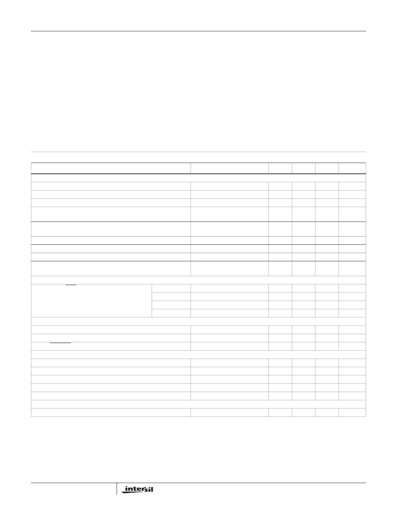
�Electrical� Specifications�
�V+� =� +5V,� V-� =� -5V,� T� A� =� +25� o� C,� f� CLK� Set� for� 3� Readings/s,� Unless� Otherwise� Specified�
�PARAMETER�
�TEST� CONDITIONS�
�MIN�
�TYP�
�MAX�
�UNITS�
�ANALOG� (Notes� 3,� 4)�
�Zero� Input� Reading�
�Ratiometric� Error� (Note� 4)�
�Linearity� Over� ±� Full� Scale� (Error� of� Reading� from� Best� Straight� Line)�
�Differential� Linearity� (Difference� Between� Worse� Case� Step� of�
�Adjacent� Counts� and� Ideal� Step)�
�Rollover� Error� (Difference� in� Reading� for� Equal� Positive� and�
�Negative� Voltage� Near� Full� Scale)�
�Noise� (Peak-to-Peak� Value� Not� Exceeded� 95%� of� Time),� e� N�
�Input� Leakage� Current,� I� ILK�
�Zero� Reading� Drift� (Note� 7)�
�Scale� Factor� Temperature� Coefficient,� T� C� (Notes� 5� and� 7)�
�V� lN� =� 0V,� V� REF� =� 1.000V�
�V� lN� =� V� REF� =� 1.000V�
�-2V� ≤� V� IN� ≤� +2V�
�-2V� ≤� V� IN� ≤� +2V�
�-V� lN� ≡� +V� lN� ≈� 2V�
�V� lN� =� 0V,� Full� scale� =� 2.000V�
�V� lN� =� 0V�
�V� lN� =� 0V,� 0� o� C� to� +70� o� C�
�V� lN� =� +2V,� 0� o� C� to� +70� o� C�
�Ext.� Ref.� 0ppm/� o� C�
�-00000�
�-3�
�-�
�-�
�-�
�-�
�-�
�-�
�-�
�+00000�
�0�
�0.5�
�0.01�
�0.5�
�15�
�1�
�0.5�
�2�
�+00000�
�+3�
�1�
�-�
�1�
�-�
�10�
�2�
�5�
�Counts�
�Counts�
�LSB�
�LSB�
�LSB�
�μ� V�
�pA�
�μ� V/� o� C�
�ppm/� o� C�
�DIGITAL� INPUTS�
�Clock� In,� Run/Hold� (See� Figure� 2)�
�V� INH�
�V� INL�
�2.8�
�-�
�2.2�
�1.6�
�-�
�0.8�
�V�
�V�
�I� INL�
�I� INH�
�V� IN� =� 0V�
�V� IN� =� +5V�
�-�
�-�
�0.02�
�0.1�
�0.1�
�10�
�mA�
�μ� A�
�DIGITAL� OUTPUTS�
�All� Outputs,� V� OL�
�B1,� B2,� B4,� B8,� D1,� D2,� D3,� D4,� D5,� V� OH�
�BUSY,� STROBE,� OVERRANGE,� UNDERRANGE,� POLARITY,� V� OH�
�I� OL� =� 1.6mA�
�I� OH� =� -1mA�
�I� OH� =� -10� μ� A�
�-�
�2.4�
�4.9�
�0.25�
�4.2�
�4.99�
�0.40�
�-�
�-�
�V�
�V�
�V�
�SUPPLY�
�+5V� Supply� Range,� V+�
�-5V� Supply� Range,� V-�
�+4�
�-3�
�+5�
�-5�
�+6�
�-8�
�V�
�V�
�+5V� Supply� Current,� I+�
�-5V� Supply� Current,� I-�
�Power� Dissipation� Capacitance,� C� PD�
�f� C� =� 0�
�f� C� =� 0�
�vs� Clock� Frequency�
�-�
�-�
�-�
�1.1�
�0.8�
�40�
�3.0�
�3.0�
�-�
�mA�
�mA�
�pF�
�CLOCK�
�Clock� Frequency� (Note� 6)�
�DC�
�2000�
�1200�
�kHz�
�NOTES:�
�3.� Tested� in� 4� 1� /� 2� digit� (20.000� count)� circuit� shown� in� Figure� 3.� (Clock� frequency� 120kHz.)�
�4.� Tested� with� a� low� dielectric� absorption� integrating� capacitor,� the� 27� Ω� INT� OUT� resistor� shorted,� and� R� lNT� =� 0.� See� Component� Value� Selection� Discussion.�
�5.� The� temperature� range� can� be� extended� to� +70� o� C� and� beyond� as� long� as� the� auto-zero� and� reference� capacitors� are� increased� to� absorb� the� higher�
�leakage� of� the� ICL7135.�
�6.� This� specification� relates� to� the� clock� frequency� range� over� which� the� lCL7135� will� correctly� perform� its� various� functions� See� “Max� Clock� Frequency”�
�section� for� limitations� on� the� clock� frequency� range� in� a� system.�
�7.� Parameter� guaranteed� by� design� or� characterization.� Not� production� tested.�
�3�
�FN3093.4�
�相关PDF资料 |
PDF描述 |
|---|---|
| IDT71V25761SA166BGI8 | IC SRAM 4MBIT 166MHZ 119BGA |
| NCP623MN-50R2G | IC REG LDO 5V .15A 6-DFN |
| IDT71V25761SA166BGI | IC SRAM 4MBIT 166MHZ 119BGA |
| TAJC335M025RNJ | CAP TANT 3.3UF 25V 20% 2312 |
| NCP623MN-33R2G | IC REG LDO 3.3V .15A 6-DFN |
相关代理商/技术参数 |
参数描述 |
|---|---|
| ICL7135CPL | 制造商:未知厂家 制造商全称:未知厂家 功能描述:(283.23 k) |
| ICL7135CQI | 功能描述:模数转换器 - ADC Integrated Circuits (ICs) RoHS:否 制造商:Texas Instruments 通道数量:2 结构:Sigma-Delta 转换速率:125 SPs to 8 KSPs 分辨率:24 bit 输入类型:Differential 信噪比:107 dB 接口类型:SPI 工作电源电压:1.7 V to 3.6 V, 2.7 V to 5.25 V 最大工作温度:+ 85 C 安装风格:SMD/SMT 封装 / 箱体:VQFN-32 |
| ICL7135CQI+ | 功能描述:模数转换器 - ADC 4 1/2 Digit ADC w/ MUXd BCD Outputs RoHS:否 制造商:Texas Instruments 通道数量:2 结构:Sigma-Delta 转换速率:125 SPs to 8 KSPs 分辨率:24 bit 输入类型:Differential 信噪比:107 dB 接口类型:SPI 工作电源电压:1.7 V to 3.6 V, 2.7 V to 5.25 V 最大工作温度:+ 85 C 安装风格:SMD/SMT 封装 / 箱体:VQFN-32 |
| ICL7135CQI+T | 功能描述:模数转换器 - ADC 4 1/2 Digit ADC w/ MUXd BCD Outputs RoHS:否 制造商:Texas Instruments 通道数量:2 结构:Sigma-Delta 转换速率:125 SPs to 8 KSPs 分辨率:24 bit 输入类型:Differential 信噪比:107 dB 接口类型:SPI 工作电源电压:1.7 V to 3.6 V, 2.7 V to 5.25 V 最大工作温度:+ 85 C 安装风格:SMD/SMT 封装 / 箱体:VQFN-32 |
| ICL7135CQI-T | 功能描述:模数转换器 - ADC RoHS:否 制造商:Texas Instruments 通道数量:2 结构:Sigma-Delta 转换速率:125 SPs to 8 KSPs 分辨率:24 bit 输入类型:Differential 信噪比:107 dB 接口类型:SPI 工作电源电压:1.7 V to 3.6 V, 2.7 V to 5.25 V 最大工作温度:+ 85 C 安装风格:SMD/SMT 封装 / 箱体:VQFN-32 |
发布紧急采购,3分钟左右您将得到回复。