- 您现在的位置:买卖IC网 > PDF目录65531 > ICS663MT PLL BASED CLOCK DRIVER, 1 TRUE OUTPUT(S), 0 INVERTED OUTPUT(S), PDSO8 PDF资料下载
参数资料
| 型号: | ICS663MT |
| 元件分类: | 时钟及定时 |
| 英文描述: | PLL BASED CLOCK DRIVER, 1 TRUE OUTPUT(S), 0 INVERTED OUTPUT(S), PDSO8 |
| 封装: | 0.150 INCH, SOIC-8 |
| 文件页数: | 3/7页 |
| 文件大小: | 146K |
| 代理商: | ICS663MT |
PLL BUILDING BLOCK
MDS 663 D
3
Revision 062904
In te gr ated Circuit Systems ● 525 Ra ce Street, San Jose, CA 9512 6 ● tel (4 08) 297-1 201 ● www.icst.com
ICS663
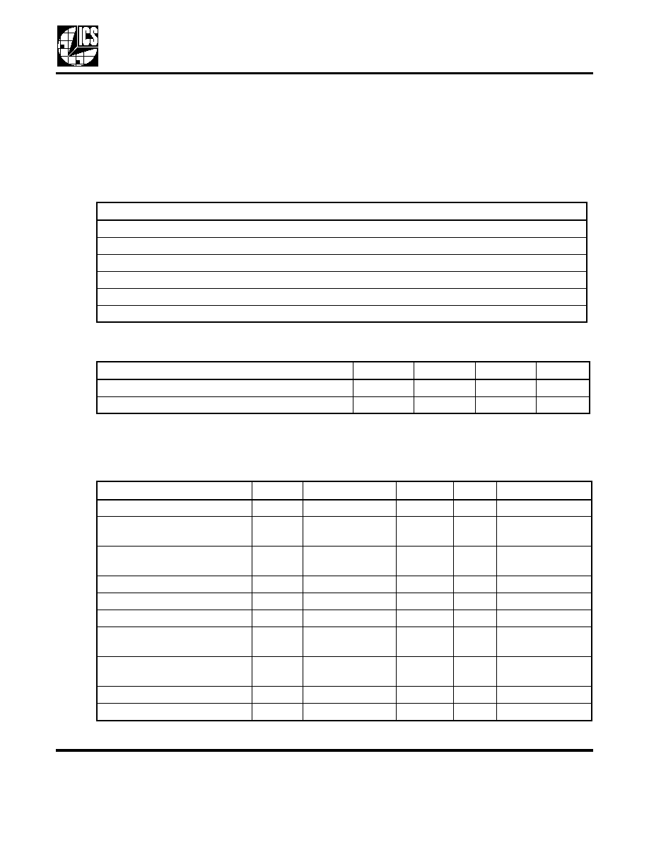
Absolute Maximum Ratings
Stresses above the ratings listed below can cause permanent damage to the ICS663. These ratings, which
are standard values for ICS commercially rated parts, are stress ratings only. Functional operation of the
device at these or any other conditions above those indicated in the operational sections of the
specifications is not implied. Exposure to absolute maximum rating conditions for extended periods can
affect product reliability. Electrical parameters are guaranteed only over the recommended operating
temperature range.
Recommended Operation Conditions
DC Electrical Characteristics
VDD=3.3 V ±5% or 5.0 V ±10%, Ambient temperature -40 to +85
°C, unless stated otherwise
Item
Rating
Supply Voltage, VDD
7V
All Inputs and Outputs
-0.5V to VDD+0.5V
Ambient Operating Temperature
0 to +70
°C
Industrial Temperature
-40 to +85
°C
Storage Temperature
-65 to +150
°C
Soldering Temperature
260
°C
Parameter
Min.
Typ.
Max.
Units
Ambient Operating Temperature
-40
+85
°C
Power Supply Voltage (measured in respect to GND)
+3.13
+5.5
V
Parameter
Symbol
Conditions
Min.
Typ.
Max.
Units
Operating Voltage
VDD
3.13
5.5
V
Logic Input High Voltage
VIH
REFIN, FBIN,
SEL
2V
Logic Input Low Voltage
VIL
REFIN, FBIN,
SEL
0.8
V
LF Input Voltage Range
VI
0VDD
V
Output High Voltage
VOH
IOH = -25 mA
2.4
V
Output Low Voltage
VOL
IOL = 25 mA
0.4
V
Output High Voltage, CMOS
level
VOH
IOH = -8 mA
VDD-0.4
Operating Supply Current
IDD
VDD = 5.0 V,
No load, 40 MHz
15
mA
Short Circuit Current
IOS
CLK
±100
mA
Input Capacitance
CI
SEL
5
pF
相关PDF资料 |
PDF描述 |
|---|---|
| ICS663M | PLL BASED CLOCK DRIVER, 1 TRUE OUTPUT(S), 0 INVERTED OUTPUT(S), PDSO8 |
| ICS664G-03LFT | 148.5 MHz, VIDEO CLOCK GENERATOR, PDSO16 |
| ICS664G-03T | 148.5 MHz, VIDEO CLOCK GENERATOR, PDSO16 |
| ICS664G-03 | 148.5 MHz, VIDEO CLOCK GENERATOR, PDSO16 |
| ICS664G-04TR | 148.5 MHz, VIDEO CLOCK GENERATOR, PDSO16 |
相关代理商/技术参数 |
参数描述 |
|---|---|
| ICS664-01 | 制造商:ICS 制造商全称:ICS 功能描述:Digital Video Clock Source |
| ICS664-02 | 制造商:ICS 制造商全称:ICS 功能描述:PECL Digital Video Clock Source |
| ICS664-03 | 制造商:ICS 制造商全称:ICS 功能描述:Digital Video Clock Source |
| ICS664-03LF | 制造商:ICS 制造商全称:ICS 功能描述:Digital Video Clock Source |
| ICS664-03LFT | 制造商:ICS 制造商全称:ICS 功能描述:Digital Video Clock Source |
发布紧急采购,3分钟左右您将得到回复。