- 您现在的位置:买卖IC网 > PDF目录67704 > ICS9148F-14 (INTEGRATED DEVICE TECHNOLOGY INC) 66.6 MHz, PROC SPECIFIC CLOCK GENERATOR, PDSO48 PDF资料下载
参数资料
| 型号: | ICS9148F-14 |
| 厂商: | INTEGRATED DEVICE TECHNOLOGY INC |
| 元件分类: | 时钟产生/分配 |
| 英文描述: | 66.6 MHz, PROC SPECIFIC CLOCK GENERATOR, PDSO48 |
| 封装: | 0.300 INCH, SSOP-48 |
| 文件页数: | 18/18页 |
| 文件大小: | 807K |
| 代理商: | ICS9148F-14 |
9
ICS9148-14
Power Management
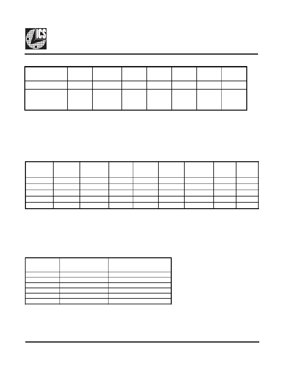
ICS9148-14 Power Management Requirements
ClockEnableConfiguration
* Off state in PD# low will be after sufficient time to allow Stop Low logic for other outputs before OSC and PLL are shutoff.
Full clock cycle timing is guaranteed at all times after the system has initially powered up except where noted. During power up
and power down operations using the PWR PD# select pin will not cause clocks of a short or longer pulse than that of the
running clock. The first clock pulse coming out of a stopped clock condition may be slightly distorted due to clock network
charging circuitry. Board routing and signal loading may have a large impact on the initial clock distortion also.
Notes.
1. Clock on latency is defined from when the clock enable goes active to when the first valid clock comes out of the device.
2. Clock off latency is defined from when the clock enable goes inactive to when the last clock is driven low out of the device.
3. Power up latency is when PD# goes inactive (high) to when the first valid clocks are output by the device. This delay is only valid in
normal (not spread spectrum) mode. Power-up from spread spectrum mode requires 10ms for valid clocks, it is recommended to keep
CPU_STOP# and PCI_STOP# low coming out of PD Low for this interval.
4. Power down has controlled clock counts applicable to CPUCLK, SDRAM, PCICLK only.
The REF and IOAPIC will be stopped independant of these.
SIGNAL
SIGNAL STATE
Latency
No. of rising edges of free
running PCICLK
CPU_ STOP#
0 (Disabled)
2
1
1 (Enabled)
1
PCI_STOP#
0 (Disabled)
2
1
1 (Enabled)
1
PWR_DWN#
1 (Normal Operation)
3
3mS
0 (Power Down)
4
2max
CPU_STOP#
PCI_STOP#
PWR_DWN#
CPUCLK
AGP,
PCICLK,
E_PCICLK
SDRAM
REF,
48/24 MHz
Crystal
OSC
VCOs
X
0
Low
Off*
0
1
Low
Running
0
1
Low
Running
1
0
1
Running
Low
Running
1
Running
Notes:
1. TCLK is a test clock driven on the X1 (crystal in pin) input during test mode.
2.AGP and PCI depend on frequency selection. For 100/33.3/66.6 will beTCLK/6 andTCLK/3 in test mode.
Select Functions
Functionality
CPU
E_PCICLK
SDRAM
REF
24 MHz
Selection
48 MHz
Selection
AGP
Tristate
HI - Z
Testmode
TCLK/2
1
TCLK/4
1,2
or
TCLK/6
1,2
TCLK/2
1
TCLK
1
TCLK/4
1
TCLK/2
1
TCLK/2
1,2
or
TCLK/3
1,2
相关PDF资料 |
PDF描述 |
|---|---|
| ICS9148F-17-LF | 100.3569 MHz, PROC SPECIFIC CLOCK GENERATOR, PDSO48 |
| ICS9148F-17 | 100.3569 MHz, PROC SPECIFIC CLOCK GENERATOR, PDSO48 |
| ICS9148F-18LF | 100 MHz, PROC SPECIFIC CLOCK GENERATOR, PDSO28 |
| ICS9148F-25 | 83.3 MHz, PROC SPECIFIC CLOCK GENERATOR, PDSO48 |
| ICS9148F-32 | 100 MHz, PROC SPECIFIC CLOCK GENERATOR, PDSO48 |
相关代理商/技术参数 |
参数描述 |
|---|---|
| ICS9148F-17 | 制造商:未知厂家 制造商全称:未知厂家 功能描述:CPU System Clock Generator |
| ICS9148F-18 | 制造商:ICS 制造商全称:ICS 功能描述:Pentium/ProTM System Clock Chip |
| ICS9148F-20 | 制造商:ICS 制造商全称:ICS 功能描述:Pentium/ProTM System Clock Chip |
| ICS9148F25 | 制造商:未知厂家 制造商全称:未知厂家 功能描述:Industrial Control IC |
| ICS9148F-25 | 功能描述:IC CLK SYNTHESIZER CHIP 48-SSOP RoHS:否 类别:集成电路 (IC) >> 时钟/计时 - 专用 系列:- 标准包装:28 系列:- 类型:时钟/频率发生器 PLL:是 主要目的:Intel CPU 服务器 输入:时钟 输出:LVCMOS 电路数:1 比率 - 输入:输出:3:22 差分 - 输入:输出:无/是 频率 - 最大:400MHz 电源电压:3.135 V ~ 3.465 V 工作温度:0°C ~ 85°C 安装类型:表面贴装 封装/外壳:64-TFSOP (0.240",6.10mm 宽) 供应商设备封装:64-TSSOP 包装:管件 |
发布紧急采购,3分钟左右您将得到回复。