- 您现在的位置:买卖IC网 > PDF目录67707 > ICS950104YFT 166 MHz, PROC SPECIFIC CLOCK GENERATOR, PDSO48 PDF资料下载
参数资料
| 型号: | ICS950104YFT |
| 元件分类: | 时钟产生/分配 |
| 英文描述: | 166 MHz, PROC SPECIFIC CLOCK GENERATOR, PDSO48 |
| 封装: | 0.300 INCH, MO-118, SSOP-48 |
| 文件页数: | 1/19页 |
| 文件大小: | 222K |
| 代理商: | ICS950104YFT |
Integrated
Circuit
Systems, Inc.
ICS950104
Third party brands and names are the property of their respective owners.
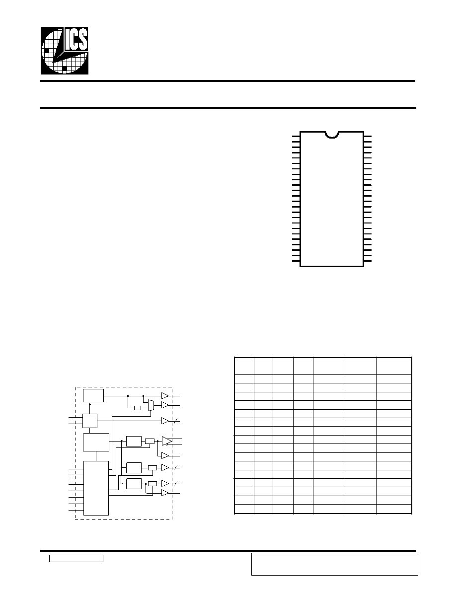
Block Diagram
950104 Rev - 09/11/01
Functionality
Pin Configuration
48-Pin 300mil SSOP
Recommended Application:
SIS630ST style chipset
Output Features:
1 - CPU clocks @ 2.5V
1 - Pair of differential CPU clocks @ 3.3V
9 - SDRAM @ 3.3V
7 - PCI @3.3V
1 - 48MHz, @3.3V
1 - 24/48MHz @ 3.3V
3 - REF @3.3V, (selectable strength) through I
2C
Features:
Programmable ouput frequency
Programmable ouput rise/fall time
Programmable CPU, SDRAM, and PCI skew
Real time system reset output
Spread spectrum for EMI control typically
by 7dB to 8dB, with programmable spread percentage
Watchdog timer technology to reset system
if over-clocking causes malfunction
Uses external 14.318MHz crystal
Skew Specifications:
CPU - CPU: <250ps
PCI - PCI: <500ps
SDRAM - SDRAM: <250ps
CPU - SDRAM:<350ps
CPU - PCI: <3ns
Programmable System Clock Chip for PIII Processor
Notes:
REF0 can be 1X or 2X strength controlled by I
2C.
* Internal Pull-up Resistor of 120K to VDD
** Internal Pull-down of 120K to GND
PLL2
PLL1
Spread
Spectrum
48MHz
24_48MHz
PCICLK (5:0)
PCICLK_F
X1
X2
XTAL
OSC
CPU
DIVDER
PCI
DIVDER
Stop
SDATA
SCLK
FS(3:0)
PD#
PCI_STOP#
CPU_STOP#
MODE
MULTSEL
Control
Logic
Config.
Reg.
/ 2
REF(2:0)
CPUCLK
SDRAM (9:0)
SDRAM
DIVDER
Stop
10
6
3
CPUCLKT0
CPUCLKC0
Stop
Advance Information
ADVANCE INFORMATION documents contain information on products
in the formative or design phase development. Characteristic data and
other specifications are design goals. ICS reserves the right to change or
discontinue these products without notice.
CPUCLKC0
CPUCLKT0
VDDCPU
GND
AVDD
X1
X2
**FS0/REF0
VDDREF
**FS1/REF1
REF2
GND
*FS2/PCICLK_F
PCICLK0
PCICLK1
PCICLK2
GND
VDDPCI
PCICLK3
PCICLK4
PCICLK5
AVDD48
**MULTSEL/24_48MHz
**FS3/48MHz
GND
IREF
GND
CPUCLK
VDDL
SDATA
SDRAM_STOP#
SDRAM0
SDRAM1
SDRAM2
SDRAM3
VDD
GND
SDRAM4
SDRAM5
SDRAM6
SDRAM7
GND
VDD
PCI_STOP#
CPU_STOP#
PD#/Vtt_PWRGD
SCLK
GND
*
#*
ICS950104
1
2
3
4
5
6
7
8
9
10
11
12
13
14
15
16
17
18
19
20
21
22
23
24
48
47
46
45
44
43
42
41
40
39
38
37
36
35
34
33
32
31
30
29
28
27
26
25
3
S
F2
S
F1
S
F0
S
F
U
P
C
)
z
H
M
(
M
A
R
D
S
)
z
H
M
(
K
L
C
I
C
P
)
z
H
M
(
00
0
6
.
6
60
.
0
13
.
3
00
0
1
0
.
0
10
.
0
13
.
3
00
1
0
.
0
5
10
.
0
15
.
7
3
00
1
3
.
3
10
.
0
13
.
3
01
0
8
.
6
66
.
3
14
.
3
01
0
1
0
.
0
13
.
3
13
.
3
0110
0
.
0
10
.
0
5
15
.
7
3
011
1
3
.
3
13
.
3
13
.
3
10
0
8
.
6
68
.
6
64
.
3
10
0
1
0
.
7
90
.
7
93
.
2
3
10
1
0
.
0
70
.
5
0
10
.
5
3
10
1
0
.
5
90
.
5
97
.
1
3
110
0
.
5
97
.
6
2
17
.
1
3
110
1
0
.
2
1
10
.
2
1
13
.
7
3
11
1
0
.
7
93
.
9
2
12
.
2
3
11
1
2
.
6
92
.
6
91
.
2
3
相关PDF资料 |
PDF描述 |
|---|---|
| ICS950201YFT | 200 MHz, PROC SPECIFIC CLOCK GENERATOR, PDSO56 |
| ICS950201YFT | 200 MHz, PROC SPECIFIC CLOCK GENERATOR, PDSO56 |
| ICS950201YF-T | 200 MHz, PROC SPECIFIC CLOCK GENERATOR, PDSO56 |
| ICS950201YGLF-T | 200 MHz, PROC SPECIFIC CLOCK GENERATOR, PDSO56 |
| ICS950201YFLF-T | 200 MHz, PROC SPECIFIC CLOCK GENERATOR, PDSO56 |
相关代理商/技术参数 |
参数描述 |
|---|---|
| ICS950201 | 制造商:ICS 制造商全称:ICS 功能描述:Programmable Timing Control Hub⑩ for P4⑩ |
| ICS950201AFLF | 功能描述:IC TIMING CTRL HUB P4 56-SSOP RoHS:是 类别:集成电路 (IC) >> 时钟/计时 - 专用 系列:TCH™ 标准包装:1 系列:- 类型:时钟/频率发生器,多路复用器 PLL:是 主要目的:存储器,RDRAM 输入:晶体 输出:LVCMOS 电路数:1 比率 - 输入:输出:1:2 差分 - 输入:输出:无/是 频率 - 最大:400MHz 电源电压:3 V ~ 3.6 V 工作温度:0°C ~ 85°C 安装类型:表面贴装 封装/外壳:16-TSSOP(0.173",4.40mm 宽) 供应商设备封装:16-TSSOP 包装:Digi-Reel® 其它名称:296-6719-6 |
| ICS950201AFLFT | 功能描述:IC TIMING CTRL HUB P4 56-SSOP RoHS:是 类别:集成电路 (IC) >> 时钟/计时 - 专用 系列:TCH™ 标准包装:28 系列:- 类型:时钟/频率发生器 PLL:是 主要目的:Intel CPU 服务器 输入:时钟 输出:LVCMOS 电路数:1 比率 - 输入:输出:3:22 差分 - 输入:输出:无/是 频率 - 最大:400MHz 电源电压:3.135 V ~ 3.465 V 工作温度:0°C ~ 85°C 安装类型:表面贴装 封装/外壳:64-TFSOP (0.240",6.10mm 宽) 供应商设备封装:64-TSSOP 包装:管件 |
| ICS950201AFT-IB0 | 制造商:Ics 功能描述:ELECTRONIC COMPONENT 制造商:Integrated Device Technology Inc 功能描述:ELECTRONIC COMPONENT |
| ICS950201AG | 制造商:INT_CIR_SYS 功能描述: |
发布紧急采购,3分钟左右您将得到回复。