- 您现在的位置:买卖IC网 > PDF目录67707 > ICS950813YFT (INTEGRATED DEVICE TECHNOLOGY INC) 200 MHz, PROC SPECIFIC CLOCK GENERATOR, PDSO56 PDF资料下载
参数资料
| 型号: | ICS950813YFT |
| 厂商: | INTEGRATED DEVICE TECHNOLOGY INC |
| 元件分类: | 时钟产生/分配 |
| 英文描述: | 200 MHz, PROC SPECIFIC CLOCK GENERATOR, PDSO56 |
| 封装: | 0.300 INCH, MO-118, SSOP-56 |
| 文件页数: | 16/22页 |
| 文件大小: | 253K |
| 代理商: | ICS950813YFT |
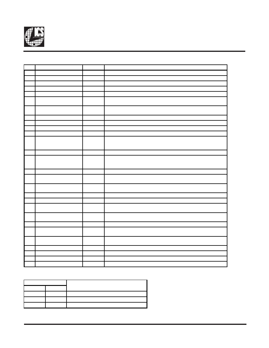
3
ICS950813
Advance Information
0708—10/10/02
Pin Description (Continued)
PIN # PIN NAME
PIN TYPE
DESCRIPTION
29
SDATA
I/O
Data pin for I2C circuitry 5V tolerant
30
SCLK
IN
Clock pin of I2C circuitry 5V tolerant
31
GND
PWR
Ground pin.
32
VDD3V66
PWR
Power pin for the 3V66 clocks.
33
3V66_0/FS4**
I/O
Frequency select latch input pin / 3.3V 66.66MHz clock output.
34
PCI_STOP#*
IN
Stops all PCICLKs besides the PCICLK_F clocks at logic 0 level, when input
low
35
3V66_1/VCH_CLK/FS3**
I/O
Frequency select latch input pin / 3.3V 66.66MHz clock output / 48MHz
VCH clock output.
36
GND
PWR
Ground pin.
37
VDD48
PWR
Power for 24 & 48MHz output buffers and fixed PLL core.
38
48MHz_DOT
OUT
48MHz clock output.
39
48MHz_USB/FS2**
I/O
Frequency select latch input pin / 3.3V 48MHz clock output.
40
PWRSAVE#*
IN
Real Time input pin to change frequency to under-clock entries located in
FS 4:2 = '100'. Clock groups gear ratio will not be change during this
operation.
41
GND
PWR
Ground pin.
42
IREF
OUT
This pin establishes the reference current for the CPUCLK pairs. This pin
requires a fixed precision resistor tied to ground in order to establish the
appropriate current.
43
MULTSEL*
IN
3.3V LVTTL input for selection the current multiplier for CPU outputs
44
CPUCLKC2
OUT
"Complementary" clocks of differential pair CPU outputs. These are current
mode outputs. External resistors are required for voltage bias.
45
CPUCLKT2
OUT
"True" clocks of differential pair CPU outputs. These are current mode
outputs. External resistors are required for voltage bias.
46
VDDCPU
PWR
Supply for CPU clocks, 3.3V nominal
47
GND
PWR
Ground pin.
48
CPUCLKC1
OUT
"Complementary" clocks of differential pair CPU outputs. These are current
mode outputs. External resistors are required for voltage bias.
49
CPUCLKT1
OUT
"True" clocks of differential pair CPU outputs. These are current mode
outputs. External resistors are required for voltage bias.
50
VDDCPU
PWR
Supply for CPU clocks, 3.3V nominal
51
CPUCLKC0
OUT
"Complementary" clocks of differential pair CPU outputs. These are current
mode outputs. External resistors are required for voltage bias.
52
CPUCLKT0
OUT
"True" clocks of differential pair CPU outputs. These are current mode
outputs. External resistors are required for voltage bias.
53
CPU_STOP#*
IN
Stops all CPUCLK besides the free running clocks
54
FS0
IN
Frequency select pin.
55
FS1
IN
Frequency select pin.
56
REF
OUT
14.318 MHz reference clock.
Power Supply
VDD
GND
1
4
Xtal, Ref, CPU PLL, digital
37
36
48MHz, Fix Digital, Fix Analog
46
47
Master clock, CPU Analog
Pin Number
Description
相关PDF资料 |
PDF描述 |
|---|---|
| ICS950902YFLF-T | 200.4 MHz, PROC SPECIFIC CLOCK GENERATOR, PDSO56 |
| ICS950902YGLF-T | 200.4 MHz, PROC SPECIFIC CLOCK GENERATOR, PDSO56 |
| ICS950902YGT | 200.4 MHz, PROC SPECIFIC CLOCK GENERATOR, PDSO56 |
| ICS950908YG-T | 200.4 MHz, PROC SPECIFIC CLOCK GENERATOR, PDSO56 |
| ICS951402YG-T | 210 MHz, PROC SPECIFIC CLOCK GENERATOR, PDSO48 |
相关代理商/技术参数 |
参数描述 |
|---|---|
| ICS950813YGT | 制造商:ICS 制造商全称:ICS 功能描述:Frequency Generator with 200MHz Differential CPU Clocks |
| ICS950818 | 制造商:ICS 制造商全称:ICS 功能描述:Frequency Generator with 200MHz Differential CPU Clocks |
| ICS950818YG-T | 制造商:ICS 制造商全称:ICS 功能描述:Frequency Generator with 200MHz Differential CPU Clocks |
| ICS950901 | 制造商:ICS 制造商全称:ICS 功能描述:Programmable Timing Control Hub for P4 |
| ICS950901YFLFT | 制造商:ICS 制造商全称:ICS 功能描述:Programmable Timing Control Hub for P4 |
发布紧急采购,3分钟左右您将得到回复。