- 您现在的位置:买卖IC网 > PDF目录3959 > IDT70T659S10BC (IDT, Integrated Device Technology Inc)IC SRAM 4MBIT 10NS 256BGA PDF资料下载
参数资料
| 型号: | IDT70T659S10BC |
| 厂商: | IDT, Integrated Device Technology Inc |
| 文件页数: | 8/27页 |
| 文件大小: | 0K |
| 描述: | IC SRAM 4MBIT 10NS 256BGA |
| 标准包装: | 6 |
| 格式 - 存储器: | RAM |
| 存储器类型: | SRAM - 双端口,异步 |
| 存储容量: | 4.5M(128K x 36) |
| 速度: | 10ns |
| 接口: | 并联 |
| 电源电压: | 2.4 V ~ 2.6 V |
| 工作温度: | 0°C ~ 70°C |
| 封装/外壳: | 256-LBGA |
| 供应商设备封装: | 256-CABGA(17x17) |
| 包装: | 托盘 |
| 其它名称: | 70T659S10BC |
第1页第2页第3页第4页第5页第6页第7页当前第8页第9页第10页第11页第12页第13页第14页第15页第16页第17页第18页第19页第20页第21页第22页第23页第24页第25页第26页第27页
�� �
�
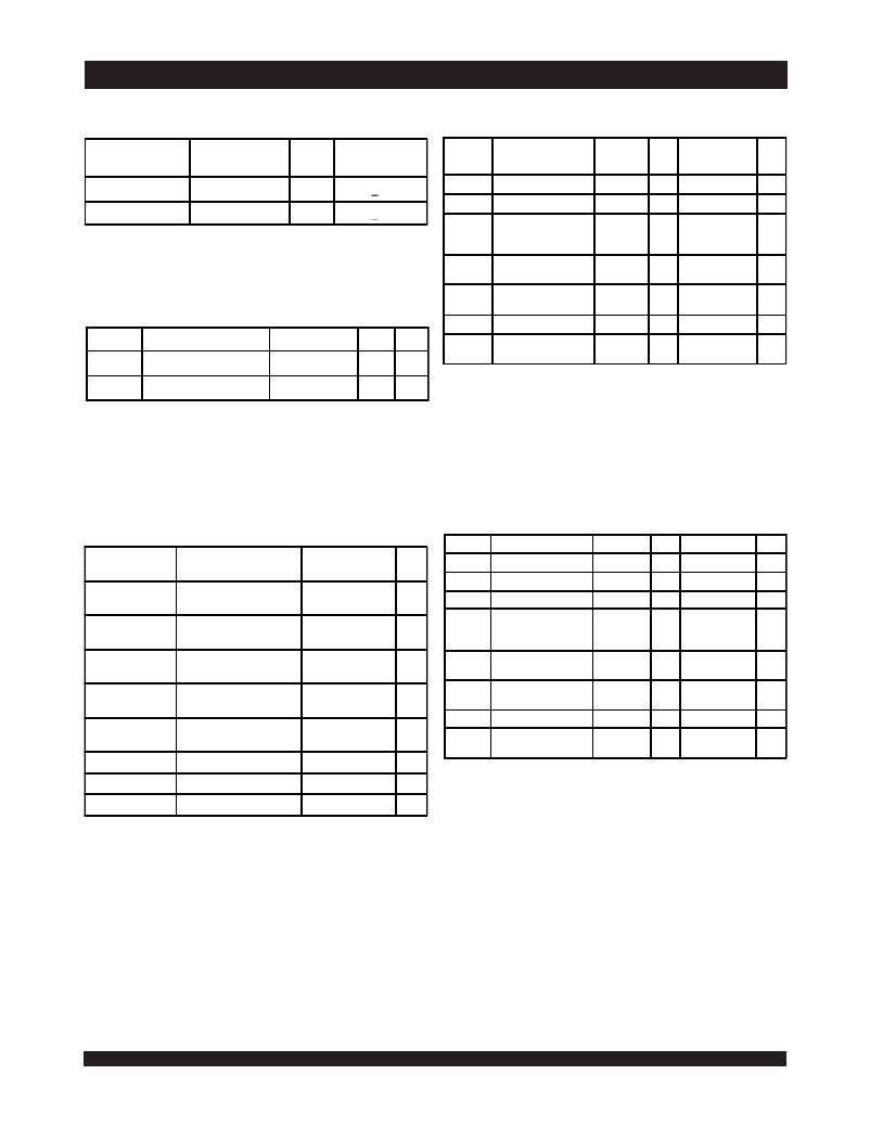
�IDT70T651/9S�
�High-Speed� 2.5V� 256/128K� x� 36� Asynchronous� Dual-Port� Static� RAM�
�Industrial� and� Commercial� Temperature� Ranges�
�Recommended� Operating�
�Temperature� and� Supply� Voltage� (1)�
�Recommended� DC� Operating�
�Conditions� with� V� DDQ� at� 2.5V�
�Ambient�
�Symbol�
�Parameter�
�Min.�
�Typ.�
�Max.�
�Unit�
�Grade�
�Temperature�
�GND�
�V� DD�
�V� DD�
�Core� Supply� Voltage�
�2.4�
�2.5�
�2.6�
�V�
�Commercial�
�Industrial�
�0� O� C� to� +70� O� C�
�-40� O� C� to� +85� O� C�
�0V�
�0V�
�2.5V� +� 100mV�
�2.5V� +� 100mV�
�V� DDQ�
�V� SS�
�I/O� Supply� Voltage�
�Ground�
�Input� High� Volltage�
�(3)�
�2.4�
�0�
�2.5�
�0�
�2.6�
�0�
�V�
�V�
�NOTE:�
�5632� tbl� 04�
�V� IH�
�(Address,� Control� &�
�Data� I/O� Inputs)� (3)�
�1.7�
�____�
�V� DDQ� +� 100mV� (2)�
�V�
�1.� This� is� the� parameter� TA.� This� is� the� "instant� on"� case� temperature.�
�V� IH�
�Input� High� Voltage�
�JTAG�
�_�
�1.7�
�____�
�V� DD� +� 100mV� (2)�
�V�
�Capacitance� (1)�
�(T� A� =� +25°C,� F� =� 1.0MH� Z� )� PQFP� ONLY�
�V� IH�
�V� IL�
�Input� High� Voltage� -�
�ZZ,� OPT,� M/� S�
�Input� Low� Voltage�
�V� DD� -� 0.2V�
�-0.3� (1)�
�____�
�____�
�V� DD� +� 100mV� (2)�
�0.7�
�V�
�V�
�Symbol�
�C� IN�
�Parameter�
�Input� Capacitance�
�Conditions� (2)�
�V� IN� =� 3dV�
�Max.�
�8�
�Unit�
�pF�
�V� IL�
�Input� Low� Voltage� -�
�ZZ,� OPT,� M/� S�
�-0.3� (1)�
�____�
�0.2�
�V�
�5632� tbl� 05�
�C� OUT� (3)�
�Output� Capacitance�
�V� OUT� =� 3dV�
�10.5�
�pF�
�NOTES:�
�1.� V� IL� (min.)� =� -1.0V� for� pulse� width� less� than� t� RC� /2� or� 5ns,� whichever� is� less.�
�5632� tbl� 08�
�NOTES:�
�1.� These� parameters� are� determined� by� device� characterization,� but� are� not�
�production� tested.�
�2.� 3dV� references� the� interpolated� capacitance� when� the� input� and� output� switch�
�from� 0V� to� 3V� or� from� 3V� to� 0V.�
�3.� C� OUT� also� references� C� I/O� .�
�2.� V� IH� (max.)� =� V� DDQ� +� 1.0V� for� pulse� width� less� than� t� RC� /2� or� 5ns,� whichever� is�
�less.�
�3.� To� select� operation� at� 2.5V� levels� on� the� I/Os� and� controls� of� a� given� port,� the�
�OPT� pin� for� that� port� must� be� set� to� V� SS� (0V),� and� V� DDQX� for� that� port� must� be�
�supplied� as� indicated� above.�
�Absolute� Maximum� Ratings� (1)�
�Recommended� DC� Operating�
�Conditions� with� V� DDQ� at� 3.3V�
�Symbol� Parameter� Min.� Typ.� Max.�
�Unit�
�Symbol�
�V� TERM�
�(V� DD� )�
�V� TERM� (2)�
�(V� DDQ� )�
�Rating�
�V� DD� Terminal� Voltage�
�with� Respect� to� GND�
�V� DDQ� Terminal� Voltage�
�with� Respect� to� GND�
�Commercial�
�&� Industrial�
�-0.5� to� 3.6�
�-0.3� to� V� DDQ� +� 0.3�
�Unit�
�V�
�V�
�V� DD�
�V� DDQ�
�V� SS�
�V� IH�
�Core� Supply� Voltage�
�I/O� Supply� Voltage� (3)�
�Ground�
�Input� High� Voltage�
�(Address,� Control�
�&Data� I/O� Inputs)� (3)�
�2.4�
�3.15�
�0�
�2.0�
�2.5�
�3.3�
�0�
�____�
�2.6�
�3.45�
�0�
�V� DDQ� +� 150mV� (2)�
�V�
�V�
�V�
�V�
�V� TERM(2)�
�(INPUTS� and� I/O's)�
�Input� and� I/O� Terminal�
�Voltage� with� Respect� to� GND�
�-0.3� to� V� DDQ� +� 0.3�
�V�
�V� IH�
�Input� High� Voltage�
�JTAG�
�_�
�1.7�
�____�
�V� DD� +� 100mV� (2)�
�V�
�-0.3�
�T� BIAS� (3)�
�T� STG�
�Temperature�
�Under� Bias�
�Storage�
�Temperature�
�-55� to� +125�
�-65� to� +150�
�o�
�o�
�C�
�C�
�V� IH�
�V� IL�
�V� IL�
�Input� High� Voltage� -�
�ZZ,� OPT,� M/� S�
�Input� Low� Voltage�
�Input� Low� Voltage� -�
�ZZ,� OPT,� M/� S�
�V� DD� -� 0.2V�
�-0.3� (1)�
�(1)�
�____�
�____�
�____�
�V� DD� +� 100mV� (2)�
�0.8�
�0.2�
�V�
�V�
�V�
�T� JN�
�Junction� Temperature�
�+150�
�o�
�C�
�5632� tbl� 06�
�I� OUT� (For� V� DDQ� =� 3.3V)� DC� Output� Current�
�I� OUT� (For� V� DDQ� =� 2.5V)� DC� Output� Current�
�50�
�40�
�mA�
�mA�
�NOTES:�
�1.� V� IL� (min.)� =� -1.0V� for� pulse� width� less� than� t� RC� /2� or� 5ns,� whichever� is� less.�
�2.� V� IH� (max.)� =� V� DDQ� +� 1.0V� for� pulse� width� less� than� t� RC� /2� or� 5ns,� whichever� is�
�5632� tbl� 07�
�NOTES:�
�1.� Stresses� greater� than� those� listed� under� ABSOLUTE� MAXIMUM� RATINGS�
�may� cause� permanent� damage� to� the� device.� This� is� a� stress� rating� only� and�
�functional� operation� of� the� device� at� these� or� any� other� conditions� above� those�
�indicated� in� the� operational� sections� of� this� specification� is� not� implied.� Exposure�
�to� absolute� maximum� rating� conditions� for� extended� periods� may� affect�
�reliability.�
�2.� This� is� a� steady-state� DC� parameter� that� applies� after� the� power� supply� has�
�reached� its� nominal� operating� value.� Power� sequencing� is� not� necessary;�
�however,� the� voltage� on� any� Input� or� I/O� pin� cannot� exceed� V� DDQ� during� power�
�supply� ramp� up.�
�3.� Ambient� Temperature� under� DC� Bias.� No� AC� Conditions.� Chip� Deselected.�
�8�
�less.�
�3.� To� select� operation� at� 3.3V� levels� on� the� I/Os� and� controls� of� a� given� port,� the�
�OPT� pin� for� that� port� must� be� set� to� V� DD� (2.5V),� and� V� DDQX� for� that� port� must� be�
�supplied� as� indicated� above.�
�相关PDF资料 |
PDF描述 |
|---|---|
| IDT70T631S10BC | IC SRAM 4MBIT 10NS 256BGA |
| IDT70V659S15DR | IC SRAM 4MBIT 15NS 208QFP |
| 306-006-525-101 | CONN CARD EDGE 6POS .156 GREEN |
| 306-006-521-104 | CONN CARD EDGE 6POS .156 GREEN |
| 306-006-521-102 | CONN CARD EDGE 6POS .156 GREEN |
相关代理商/技术参数 |
参数描述 |
|---|---|
| IDT70T659S10BC8 | 功能描述:IC SRAM 4MBIT 10NS 256BGA RoHS:否 类别:集成电路 (IC) >> 存储器 系列:- 标准包装:3,000 系列:- 格式 - 存储器:EEPROMs - 串行 存储器类型:EEPROM 存储容量:8K (1K x 8) 速度:400kHz 接口:I²C,2 线串口 电源电压:1.7 V ~ 5.5 V 工作温度:-40°C ~ 85°C 封装/外壳:8-SOIC(0.154",3.90mm 宽) 供应商设备封装:8-SOIC 包装:带卷 (TR) |
| IDT70T659S10BCI | 功能描述:IC SRAM 4MBIT 10NS 256BGA RoHS:否 类别:集成电路 (IC) >> 存储器 系列:- 标准包装:3,000 系列:- 格式 - 存储器:EEPROMs - 串行 存储器类型:EEPROM 存储容量:8K (1K x 8) 速度:400kHz 接口:I²C,2 线串口 电源电压:1.7 V ~ 5.5 V 工作温度:-40°C ~ 85°C 封装/外壳:8-SOIC(0.154",3.90mm 宽) 供应商设备封装:8-SOIC 包装:带卷 (TR) |
| IDT70T659S10BCI8 | 功能描述:IC SRAM 4MBIT 10NS 256BGA RoHS:否 类别:集成电路 (IC) >> 存储器 系列:- 标准包装:3,000 系列:- 格式 - 存储器:EEPROMs - 串行 存储器类型:EEPROM 存储容量:8K (1K x 8) 速度:400kHz 接口:I²C,2 线串口 电源电压:1.7 V ~ 5.5 V 工作温度:-40°C ~ 85°C 封装/外壳:8-SOIC(0.154",3.90mm 宽) 供应商设备封装:8-SOIC 包装:带卷 (TR) |
| IDT70T659S10BF | 功能描述:IC SRAM 4MBIT 10NS 208FBGA RoHS:否 类别:集成电路 (IC) >> 存储器 系列:- 标准包装:3,000 系列:- 格式 - 存储器:EEPROMs - 串行 存储器类型:EEPROM 存储容量:8K (1K x 8) 速度:400kHz 接口:I²C,2 线串口 电源电压:1.7 V ~ 5.5 V 工作温度:-40°C ~ 85°C 封装/外壳:8-SOIC(0.154",3.90mm 宽) 供应商设备封装:8-SOIC 包装:带卷 (TR) |
| IDT70T659S10BF8 | 功能描述:IC SRAM 4MBIT 10NS 208FBGA RoHS:否 类别:集成电路 (IC) >> 存储器 系列:- 标准包装:3,000 系列:- 格式 - 存储器:EEPROMs - 串行 存储器类型:EEPROM 存储容量:8K (1K x 8) 速度:400kHz 接口:I²C,2 线串口 电源电压:1.7 V ~ 5.5 V 工作温度:-40°C ~ 85°C 封装/外壳:8-SOIC(0.154",3.90mm 宽) 供应商设备封装:8-SOIC 包装:带卷 (TR) |
发布紧急采购,3分钟左右您将得到回复。