- 您现在的位置:买卖IC网 > PDF目录299200 > IDT7140SA35JG (INTEGRATED DEVICE TECHNOLOGY INC) HIGH SPEED 1K X 8 DUAL-PORT STATIC SRAM PDF资料下载
参数资料
| 型号: | IDT7140SA35JG |
| 厂商: | INTEGRATED DEVICE TECHNOLOGY INC |
| 元件分类: | SRAM |
| 英文描述: | HIGH SPEED 1K X 8 DUAL-PORT STATIC SRAM |
| 中文描述: | 1K X 8 DUAL-PORT SRAM, 35 ns, PQCC52 |
| 封装: | 0.750 X 0.750 INCH, 0.170 INCH HEIGHT, GREEN, PLASTIC, LCC-52 |
| 文件页数: | 9/19页 |
| 文件大小: | 149K |
| 代理商: | IDT7140SA35JG |
17
IDT7130SA/LA and IDT7140SA/LA
High-Speed 1K x 8 Dual-Port Static SRAM
Military, Industrial and Commercial Temperature Ranges
Functional Description
The IDT7130/IDT7140 provides two ports with separate control,
address and I/O pins that permit independent access for reads or
writes to any location in memory. The IDT7130/IDT7140 has an
automatic power down feature controlled by
CE. The CE controls on-
chip power down circuitry that permits the respective port to go into a
standby mode when not selected (
CE = VIH). When a port is enabled,
access to the entire memory array is permitted.
Interrupts
If the user chooses the interrupt function, a memory location (mail
box or message center) is assigned to each port. The left port interrupt
flag (
INTL) is asserted when the right port writes to memory location
3FE (HEX), where a write is defined as the
CER = R/WR = VILper Truth
Table II. The left port clears the interrupt by access address location
3FE access when
CEL = OEL =VIL, R/W is a "don't care". Likewise, the
right port interrupt flag (
INTR) is asserted when the left port writes to
memory location 3FF (HEX) and to clear the interrupt flag (
INTR), the
right port must access the memory location 3FF. The message (8 bits)
at 3FE or 3FF is user-defined, since it is an addressable SRAM
location. If the interrupt function is not used, address locations 3FE and
3FF are not used as mail boxes, but as part of the random access
memory. Refer to Truth Table II for the interrupt operation.
Busy Logic
Busy Logic provides a hardware indication that both ports of the
RAM have accessed the same location at the same time. It also allows
one of the two accesses to proceed and signals the other side that the
RAM is “Busy”. The
BUSY pin can then be used to stall the access until
the operation on the other side is completed. If a write operation has
been attempted from the side that receives a
BUSY indication, the
write signal is gated internally to prevent the write from proceeding.
The use of
BUSY logic is not required or desirable for all applica-
tions. In some cases it may be useful to logically OR the
BUSY outputs
together and use any
BUSY indication as an interrupt source to flag the
event of an illegal or illogical operation. In slave mode the
BUSY pin
operates solely as a write inhibit input pin. Normal operation can be
programmed by tying the
BUSY pins HIGH. If desired, unintended
write operations can be prevented to a port by tying the
BUSY pin for
that port LOW.
The
BUSY outputs on the IDT7130 RAM (Master) are open drain
type outputs and require open drain resistors to operate. If these
RAMs are being expanded in depth, then the
BUSY indication for the
resulting array does not require the use of an external AND gate.
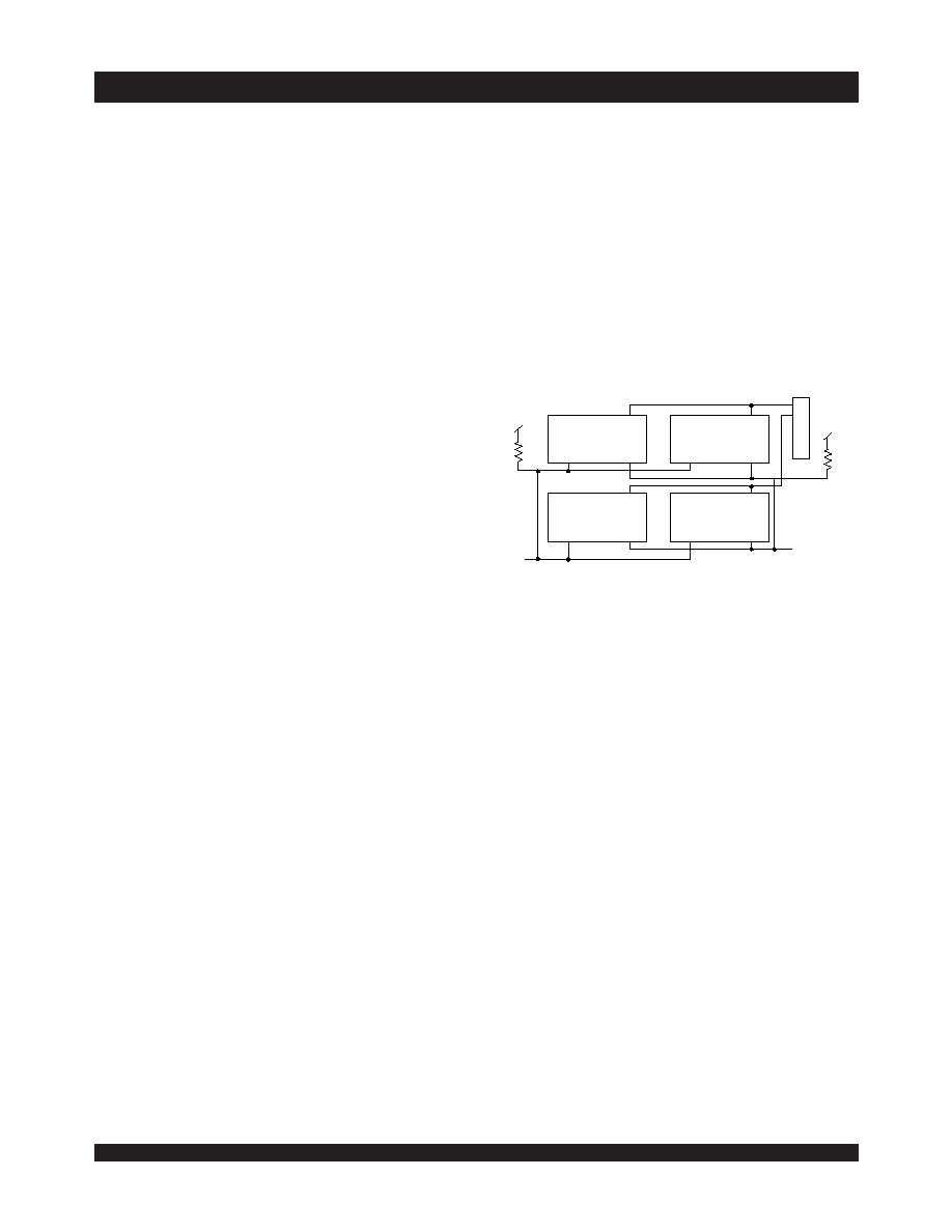
Width Expansion with Busy Logic
Master/Slave Arrays
When expanding an RAM array in width while using busy logic, one
master part is used to decide which side of the RAM array will receive
a busy indication, and to output that indication. Any number of slaves
to be addressed in the same address range as the master, use the
busy signal as a write inhibit signal. Thus on the IDT7130/IDT7140
RAMs the
BUSY pin is an output if the part is Master (IDT7130), and
the
BUSY pin is an input if the part is a Slave (IDT7140) as shown in
Figure 3.
If two or more master parts were used when expanding in width,
a split decision could result with one master indicating busy on one side
of the array and another master indicating busy on one other side of
the array. This would inhibit the write operations from one port for part
of a word and inhibit the write operations from the other port for the
other part of the word.
The
BUSY arbitration, on a Master, is based on the chip enable and
address signals only. It ignores whether an access is a read or write.
In a master/slave array, both address and chip enable must be valid
long enough for a
BUSY flag to be output from the master before the
actual write pulse can be initiated with either the R/
W signal or the byte
enables. Failure to observe this timing can result in a glitched internal
write inhibit signal and corrupted data in the slave.
Figure 3. Busy and chip enable routing for both width and depth
expansion with IDT7130 (Master) and IDT7140 (Slave)RAMs.
2689 drw 18
MASTER
Dual Port
RAM
BUSYL
BUSYR
CE
MASTER
Dual Port
RAM
BUSYL
BUSYR
CE
SLAVE
Dual Port
RAM
BUSYL
BUSYR
CE
SLAVE
Dual Port
RAM
BUSYL
BUSYR
CE
BUSYL
BUSYR
D
E
C
O
D
E
R
5V
270
270
.
相关PDF资料 |
PDF描述 |
|---|---|
| IDT7140SA35JGB | HIGH SPEED 1K X 8 DUAL-PORT STATIC SRAM |
| IDT7140SA25PG | HIGH SPEED 1K X 8 DUAL-PORT STATIC SRAM |
| IDT7140SA25PGB | HIGH SPEED 1K X 8 DUAL-PORT STATIC SRAM |
| IDT7140SA25PGI | HIGH SPEED 1K X 8 DUAL-PORT STATIC SRAM |
| IDT71589S25DB | 32K X 9 CACHE TAG SRAM, 24 ns, CDIP32 |
相关代理商/技术参数 |
参数描述 |
|---|---|
| IDT7140SA35JI | 功能描述:IC SRAM 8KBIT 35NS 52PLCC RoHS:否 类别:集成电路 (IC) >> 存储器 系列:- 标准包装:2,000 系列:MoBL® 格式 - 存储器:RAM 存储器类型:SRAM - 异步 存储容量:16M(2M x 8,1M x 16) 速度:45ns 接口:并联 电源电压:2.2 V ~ 3.6 V 工作温度:-40°C ~ 85°C 封装/外壳:48-VFBGA 供应商设备封装:48-VFBGA(6x8) 包装:带卷 (TR) |
| IDT7140SA35JI8 | 功能描述:IC SRAM 8KBIT 35NS 52PLCC RoHS:否 类别:集成电路 (IC) >> 存储器 系列:- 标准包装:2,000 系列:MoBL® 格式 - 存储器:RAM 存储器类型:SRAM - 异步 存储容量:16M(2M x 8,1M x 16) 速度:45ns 接口:并联 电源电压:2.2 V ~ 3.6 V 工作温度:-40°C ~ 85°C 封装/外壳:48-VFBGA 供应商设备封装:48-VFBGA(6x8) 包装:带卷 (TR) |
| IDT7140SA35L48B | 制造商:Integrated Device Technology Inc 功能描述:IC SRAM 8KBIT 35NS 48LCC |
| IDT7140SA35P | 功能描述:IC SRAM 8KBIT 35NS 48DIP RoHS:否 类别:集成电路 (IC) >> 存储器 系列:- 标准包装:2,000 系列:MoBL® 格式 - 存储器:RAM 存储器类型:SRAM - 异步 存储容量:16M(2M x 8,1M x 16) 速度:45ns 接口:并联 电源电压:2.2 V ~ 3.6 V 工作温度:-40°C ~ 85°C 封装/外壳:48-VFBGA 供应商设备封装:48-VFBGA(6x8) 包装:带卷 (TR) |
| IDT7140SA35PF | 功能描述:IC SRAM 8KBIT 35NS 64TQFP RoHS:否 类别:集成电路 (IC) >> 存储器 系列:- 标准包装:2,000 系列:MoBL® 格式 - 存储器:RAM 存储器类型:SRAM - 异步 存储容量:16M(2M x 8,1M x 16) 速度:45ns 接口:并联 电源电压:2.2 V ~ 3.6 V 工作温度:-40°C ~ 85°C 封装/外壳:48-VFBGA 供应商设备封装:48-VFBGA(6x8) 包装:带卷 (TR) |
发布紧急采购,3分钟左右您将得到回复。