- 您现在的位置:买卖IC网 > PDF目录10008 > IDT72261LA20TFI8 (IDT, Integrated Device Technology Inc)IC FIFO 8192X18 LP 20NS 64QFP PDF资料下载
参数资料
| 型号: | IDT72261LA20TFI8 |
| 厂商: | IDT, Integrated Device Technology Inc |
| 文件页数: | 21/27页 |
| 文件大小: | 0K |
| 描述: | IC FIFO 8192X18 LP 20NS 64QFP |
| 标准包装: | 1,250 |
| 系列: | 7200 |
| 功能: | 同步 |
| 存储容量: | 144K(8K x 18) |
| 数据速率: | 50MHz |
| 访问时间: | 20ns |
| 电源电压: | 4.5 V ~ 5.5 V |
| 工作温度: | -40°C ~ 85°C |
| 安装类型: | 表面贴装 |
| 封装/外壳: | 64-LQFP |
| 供应商设备封装: | 64-TQFP(10x10) |
| 包装: | 带卷 (TR) |
| 其它名称: | 72261LA20TFI8 |
第1页第2页第3页第4页第5页第6页第7页第8页第9页第10页第11页第12页第13页第14页第15页第16页第17页第18页第19页第20页当前第21页第22页第23页第24页第25页第26页第27页
3
COMMERCIALANDINDUSTRIAL
TEMPERATURERANGES
IDT72261LA/72271LA SuperSync FIFO
16,384 x 9 and 32,768 x 9
DESCRIPTION (CONTINUED)
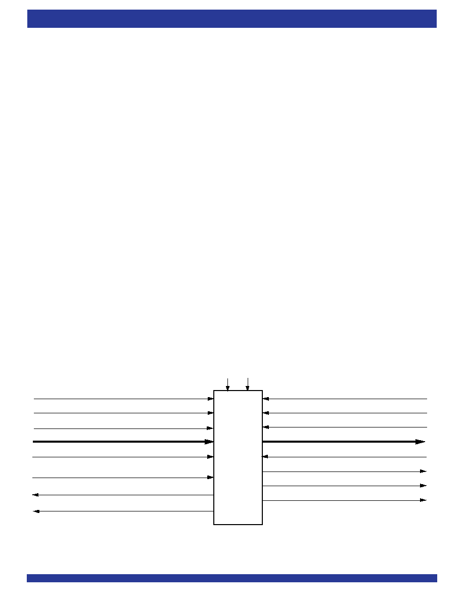
Figure 1. Block Diagram of Single 16,384 x 9 and 32,768 x 9 Synchronous FIFO
DATA OUT (Q0 - Qn)
DATA IN (D0 - Dn)
MASTER RESET (
MRS)
READ CLOCK (RCLK)
READ ENABLE (
REN)
OUTPUT ENABLE (
OE)
EMPTY FLAG/OUTPUT READY (
EF/OR)
PROGRAMMABLE ALMOST-EMPTY (
PAE)
WRITE CLOCK (WCLK)
WRITE ENABLE (
WEN)
LOAD (
LD)
FULL FLAG/INPUT READY (
FF/IR)
PROGRAMMABLE ALMOST-FULL (
PAF)
IDT
72261LA
72271LA
PARTIAL RESET (
PRS)
FIRST WORD FALL THROUGH/SERIAL INPUT
(FWFT/SI)
RETRANSMIT (
RT)
4671 drw 03
HALF FULL FLAG (
HF)
SERIAL ENABLE(
SEN)
In FWFT mode, the first word written to an empty FIFO is clocked directly
to the data output lines after three transitions of the RCLK signal. A REN
does not have to be asserted for accessing the first word. However,
subsequent words written to the FIFO do require a LOW on REN for
access. The state of the FWFT/SI input during Master Reset determines
the timing mode in use.
For applications requiring more data storage capacity than a single
FIFO can provide, the FWFT timing mode permits depth expansion by
chaining FIFOs in series (i.e. the data outputs of one FIFO are connected
to the corresponding data inputs of the next). No external logic is required.
These FIFOs have five flag pins, EF/OR (Empty Flag or Output Ready),
FF/IR (Full Flag or Input Ready), HF (Half-full Flag), PAE (Programmable
Almost-Empty flag) and PAF (Programmable Almost-Full flag). The EF
and FF functions are selected in IDT Standard mode. The IR and OR
functions are selected in FWFT mode. HF, PAE and PAF are always
available for use, irrespective of timing mode.
PAE and PAF can be programmed independently to switch at any point
in memory. (See Table I and Table II.) Programmable offsets determine
the flag switching threshold and can be loaded by two methods: parallel or
serial. Two default offset settings are also provided, so that PAE can be
set to switch at 127 or 1,023 locations from the empty boundary and the
PAF threshold can be set at 127 or 1,023 locations from the full boundary.
These choices are made with the LD pin during Master Reset.
For serial programming, SEN together with LD on each rising edge of
WCLK, are used to load the offset registers via the Serial Input (SI). For
parallel programming, WEN together with LD on each rising edge of WCLK,
areusedtoloadtheoffsetregistersviaDn. RENtogetherwithLDoneachrising
edge of RCLK can be used to read the offsets in parallel from Qn regardless
of whether serial or parallel offset loading has been selected.
DuringMasterReset(MRS)thefollowingeventsoccur:Thereadandwrite
pointers are set to the first location of the FIFO. The FWFT pin selects IDT
StandardmodeorFWFTmode. TheLDpinselectseitherapartialflagdefault
settingof127withparallelprogrammingorapartialflagdefaultsettingof1,023
withserialprogramming. Theflagsareupdatedaccordingtothetimingmode
anddefaultoffsetsselected.
The Partial Reset (PRS) also sets the read and write pointers to the first
location of the memory. However, the timing mode, partial flag program-
ming method, and default or programmed offset settings existing before
Partial Reset remain unchanged. The flags are updated according to the
timing mode and offsets in effect. PRS is useful for resetting a device in
mid-operation, when reprogramming partial flags would be undesirable.
The Retransmit function allows data to be reread from the FIFO more
than once. A LOW on the RT input during a rising RCLK edge initiates a
retransmit operation by setting the read pointer to the first location of the
memory array.
If, at any time, the FIFO is not actively performing an operation, the chip
will automatically power down. Once in the power down state, the standby
supply current consumption is minimized. Initiating any operation (by
activating control inputs) will immediately take the device out of the power
down state.
The IDT72261LA/72271LA are fabricated using high speed submicron
CMOStechnology.
相关PDF资料 |
PDF描述 |
|---|---|
| VE-2N1-IU-F4 | CONVERTER MOD DC/DC 12V 200W |
| MS27505E17F35PD | CONN RCPT 55POS BOX MNT W/PINS |
| IDT72261LA15TF8 | IC FIFO 8192X18 LP 15NS 64QFP |
| MS27473E16A26PA | CONN PLUG 26POS STRAIGHT W/PINS |
| IDT72255LA20TFI8 | IC FIFO 8KX18 LP 20NS 64QFP |
相关代理商/技术参数 |
参数描述 |
|---|---|
| IDT72265LA10PF | 功能描述:IC FIFO 8KX18 LP 10NS 64QFP RoHS:否 类别:集成电路 (IC) >> 逻辑 - FIFO 系列:7200 标准包装:90 系列:7200 功能:同步 存储容量:288K(16K x 18) 数据速率:100MHz 访问时间:10ns 电源电压:4.5 V ~ 5.5 V 工作温度:0°C ~ 70°C 安装类型:表面贴装 封装/外壳:64-LQFP 供应商设备封装:64-TQFP(14x14) 包装:托盘 其它名称:72271LA10PF |
| IDT72265LA10PF8 | 功能描述:IC FIFO 8KX18 LP 10NS 64QFP RoHS:否 类别:集成电路 (IC) >> 逻辑 - FIFO 系列:7200 标准包装:90 系列:7200 功能:同步 存储容量:288K(16K x 18) 数据速率:100MHz 访问时间:10ns 电源电压:4.5 V ~ 5.5 V 工作温度:0°C ~ 70°C 安装类型:表面贴装 封装/外壳:64-LQFP 供应商设备封装:64-TQFP(14x14) 包装:托盘 其它名称:72271LA10PF |
| IDT72265LA10PFG | 功能描述:IC FIFO SUPERSYNC 8KX18 64QFP RoHS:是 类别:集成电路 (IC) >> 逻辑 - FIFO 系列:7200 标准包装:90 系列:74ABT 功能:同步,双端口 存储容量:4.6K(64 x 36 x2) 数据速率:67MHz 访问时间:- 电源电压:4.5 V ~ 5.5 V 工作温度:0°C ~ 70°C 安装类型:表面贴装 封装/外壳:120-LQFP 裸露焊盘 供应商设备封装:120-HLQFP(14x14) 包装:托盘 产品目录页面:1005 (CN2011-ZH PDF) 其它名称:296-3984 |
| IDT72265LA10TF | 功能描述:IC FIFO 8KX18 LP 10NS 64QFP RoHS:否 类别:集成电路 (IC) >> 逻辑 - FIFO 系列:7200 标准包装:90 系列:7200 功能:同步 存储容量:288K(16K x 18) 数据速率:100MHz 访问时间:10ns 电源电压:4.5 V ~ 5.5 V 工作温度:0°C ~ 70°C 安装类型:表面贴装 封装/外壳:64-LQFP 供应商设备封装:64-TQFP(14x14) 包装:托盘 其它名称:72271LA10PF |
| IDT72265LA10TF8 | 功能描述:IC FIFO 8KX18 LP 10NS 64QFP RoHS:否 类别:集成电路 (IC) >> 逻辑 - FIFO 系列:7200 标准包装:90 系列:7200 功能:同步 存储容量:288K(16K x 18) 数据速率:100MHz 访问时间:10ns 电源电压:4.5 V ~ 5.5 V 工作温度:0°C ~ 70°C 安装类型:表面贴装 封装/外壳:64-LQFP 供应商设备封装:64-TQFP(14x14) 包装:托盘 其它名称:72271LA10PF |
发布紧急采购,3分钟左右您将得到回复。